2020-05-23
Visited : 2264
Graphenea, a world-leading graphene producer, has announced the successful completion of the G4SEMI project - integrating graphene into CMOS semiconductor workflows, funded by the European Commission SME Instrument.
Graphenea announces the successful completion of project G4SEMI, funded by the European Commission SME Instrument. The project, which lasted two years, aimed at integrating graphene into CMOS semiconductor workflows.
The business goal was to create added value through fast-tracking market acceptance of graphene-on-wafer by lowering the technological barriers to adoption of graphene by the €545 billion semiconductor devices industry.
The key challenges related to improving the technological competitiveness of graphene production to match the demands imposed by state-of-the-art processes at mass-production levels, while reducing the cost of graphene. The most immediate applications of graphene mass production are in photosensors, biosensors and memory devices.
Three key technical challenges were to increase the size of the graphene wafers on offer, scaling up graphene transfer, while further improving the quality by developing novel post-fabrication cleaning processes.
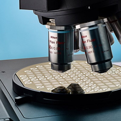
A critical step to integration into CMOS processes was scaling the size of graphene films on wafers up to 200mm, which is the minimum processing size in many semiconductor fabs – the “factories” for semiconductor devices that run today’s technology. Aside from fine-tuning graphene growth technology to reproduce the same high quality films on a scale larger than the previously largest 150mm wafers, it was pivotal to understand how to transfer such a large film from the growth substrate without introducing additional defects.
Indeed Graphenea’s research team successfully developed an alternative to the wet transfer process which greatly enhances both yield and output simultaneously, paving the way for mass production of graphene on semiconductor substrates.
Among other stringent requirements, CMOS production imposes limits on metal contamination. During project G4SEMI, Graphenea has successfully developed cleaning processes that greatly improve particle contamination levels in graphene, reducing contamination to levels acceptable by fabs.
To summarize, project G4SEMI addressed key technological challenges, making graphene production acceptable for integration into CMOS processes in today’s fabs. The project was supported by the SME Instrument of the European Commission, which supports high-risk, high-potential small and medium-sized enterprises to develop and bring to market new products, services and business models that could drive economic growth.
This project has received funding from the European Union's Horizon 2020 research and innovation programme under grant agreement No 811715.
Read the original article on Graphenea.