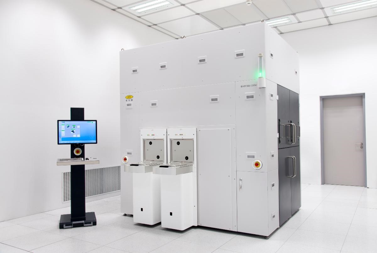
Leveraging EVG's decades of experience in hybrid bonding technology, the EVG320 D2W fills a critical need for innovative process solutions that can accelerate the deployment of heterogeneous integration and enable new generations of devices and systems such as high-bandwidth memory (HBM), logic-on-memory, chiplets, segmented and 3D system on chip (SoC) devices, and 3D stacked backside illuminated CMOS image sensors.
Hybrid Bonding is an Enabling Process for Heterogeneous Integration
Leading-edge applications such as artificial intelligence (AI), autonomous driving, augmented/virtual reality (AR/VR) and 5G require the development of high-bandwidth, high-performance and low-power-consumption devices without increasing production cost. As traditional 2D silicon scaling reaches its cost limits, the semiconductor industry is turning to heterogeneous integration -- the manufacturing, assembly and packaging of multiple different components or dies with different feature sizes and materials onto a single device or package in order to increase performance on new device generations.
Wafer-to-wafer (W2W) hybrid bonding, which involves stacking and electrically connecting wafers from different production lines, is a central process in heterogeneous integration and has a proven track record of success for certain applications such as CMOS image sensors and various memory and logic technologies. However, in cases where the components or dies are not the same size, D2W hybrid bonding offers a viable pathway to enabling heterogeneous integration. With its new D2W bonding solution, extensive experience drawn from its market-leading W2W hybrid bonding solutions and industry collaborations supported by its Heterogeneous Integration Competence Center™, EVG is well positioned to support D2W bonding applications.

EVG®320 D2W die preparation and activation system for die-to-wafer (D2W) bonding applications.
"For 20 years, EVG has continually set new standards for wafer-to-wafer hybrid and fusion bonding with the largest installed base of wafer bonding solutions worldwide," stated Paul Lindner, executive technology director of EV Group. "We have already begun serving the needs of the emerging die-to-wafer market with a dedicated version of our established EVG GEMINI® FB system specially configured for die-to-wafer bonding.
The new EVG320 D2W die preparation and activation system adds to our expertise in die-to-wafer bonding and completes EVG's equipment portfolio for providing an end-to-end hybrid bonding solution to accelerate the deployment of 3D/heterogeneous integration. In the future, we anticipate that both wafer-to-wafer and die-to-wafer process flows will be required and run in parallel in numerous fabs for heterogeneous integration applications, providing many opportunities for EVG to support this critical and rapidly growing technology landscape."
Die-to-Wafer Process Flow
Several different D2W bonding methods are available and are selected depending upon the application and customer requirements. In collective D2W (Co-D2W) bonding, singulated dies are placed on collective die carriers and then are transported to a target wafer for die transfer where a W2W hybrid or fusion bonding system, such as the GEMINI FB, are used to bond the dies to the target wafer. In direct placement D2W (DP-D2W) bonding, the singulated dies are bonded to the target wafer one by one using a pick-and-place flip-chip bonder. Plasma activation and cleaning of the surfaces of the dies on the handler wafer are essential steps for establishing a high-yielding bond and electrical interface between the dies and target wafer. This is where the EVG320 D2W activation system comes in.
Product Details
The EVG320 D2W is a highly flexible platform that features a universal hardware/software interface to enable seamless integration with third-party pick-and-place die bonding systems. It also can operate as a stand-alone system depending on integration and line balancing requirements. The system incorporates EVG's advanced cleaning and plasma activation technology, which is available across its industry-standard W2W fusion and hybrid bonding platforms and has been proven in hundreds of installed modules worldwide.
In addition, the EVG320 D2W features EVG's alignment verification module (AVM), an integrated metrology module that provides direct feedback to the die bonder on critical process parameters, such as die placement accuracy and die-height information as well as post-bond metrology, for improved process control. Additional features include flexible substrate handling that can accommodate any type of die carrier or film frame that can support plasma activation, hybrid and fusion bonding cleanliness standards, and SECS/GEM standard support.
Read the original article on Silicon Semiconductor.
