Small but profound improvements drive every generation of breakthroughs in optical telecommunications. New component materials allow devices to be smaller, more efficient, and more accurate. However, these materials work best when researchers design and build them from nanoscale building blocks. These tiny building blocks are only billionths of a meter wide. These materials offer brighter, more controlled light emission that is closer to the infrared spectrum required for telecommunications.
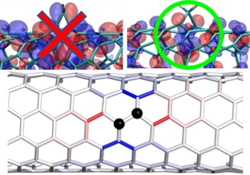
The introduction of controlled divalent bonds stabilizes the creation of potential energy wells (top), particularly along specific carbon atoms structures on the nanotube surface (bottom).
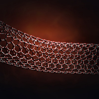
Nanotubes are hollow cylinders of hexagonally bonded carbon sheets that are only one atom thick. Their electrical, elastic, thermal, and optical properties are particularly interesting for advanced telecommunications materials. The challenge has been that single-walled carbon nanotubes tend to emit light inefficiently and at the less-useful blue end of the light wave spectrum. These factors make them less suitable for telecommunications. The inefficiency stems from the rapid movement of excited electrons (or “excitons”) across the surface of the nanotubes. These excitons decay and lose their energy as heat when they encounter natural structural defects on the surface.
Optically useful excited nanotubes must therefore minimize the production of heat, maximize light emission, and produce light closer to the infrared telecommunication-relevant spectrum. Attaching specific chemical groups to the surface of the nanotube modifies the potential energy landscape by creating “energy wells” along the surface of the nanotube. The wells attract the free-floating surface excitons and trap them in areas a few nanometers long. Because the excited electrons cannot move freely, they are “forced” to release energy as light rather than heat. The trapped excitons also have a lower energy state, which “redshifts” the emitted light waves closer to the desired infrared part of the spectrum.
In this study, scientists from the Center for Integrated Nanotechnologies, a Department of Energy (DOE) Office of Science user facility, and their co-authors tested three new types of chemical groups on single-walled carbon nanotubes. The researchers created theoretical models of atomic-scale structures that optimized the placement of stable chemical bonds to maximize the optical emission of the nanotubes. They verified the results experimentally, providing direct evidence that the modified surfaces improved light emission. This innovation will help future teams to create more finely tuned optical functions in chemically modified nanotubes.
Read the original article on U.S. Department of Energy.