Currently, most cutting-edge processes use FETs (Field Effect Transistors). As they’ve gotten smaller, we’ve added fins and other tricks to get around the fact that things get weird when they’re small. The industry is looking to move to GAAFETs (Gate All Around FET) as Intel and Samsung have declared their 3 nm processes (or equivalent) will use the new type of gate. As transistors have shrunk, the “off-state” leakage current has grown. GAAFETs are multi-gate devices, allowing better control of that leakage, among other things.
As usual, we’re already looking at what is past 3 nm towards 2 nm, and the concern is that GAAFET won’t scale past 3 nm. Carbon Nanotubes are an up-and-coming technology as they offer a few critical advantages. They conduct heat exceptionally well, exhibit higher transconductance, and conduct large amounts of power. In addition, they show higher electron mobility than conventional MOSFETs and often outperform them with less power even while being at larger sizes. This is all to say that they’re an awesome piece of tech with a few caveats.
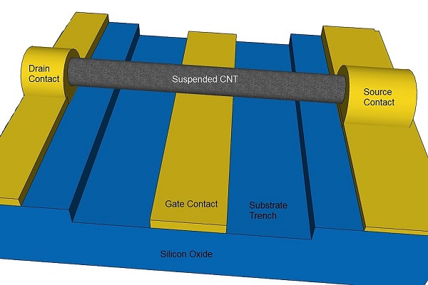
Carbon nanotube field-effect transistor.
The gotchas are mainly related to production and reliability. The current process for growing nanotubes produces a few tubes: metallic and semiconducting. For transistors, you want to use the latter rather than the former, and getting an accurately uniform mix of tubes is tricky when they’re only 1 nm wide. Additionally, once you have a uniform, high-quality tube mixture, how do you get the tubes where you want them? Each transistor will use several tubes so a single wafer uses several trillion tubes. Even at fractions of fractions of pennies, a trillion of something adds up quickly. There have been some attempts at growing the tubes on-chip, but ALD (Atomic Layer Deposition) doesn’t nucleate on carbon surfaces.
As we mentioned earlier, there are two reliability concerns. First, carbon nanotubes of this size degrade in the atmosphere, some early ICs only lasting a few weeks before a critical channel broke. Second, multi-channel transistors (where multiple tubes are used per transistor) last longer because of redundant connections.
Most players are investigating the space: IBM, Darpa, TSMC, Stanford, MIT, Intel, Nantero, and dozens of others. Right there are dozens of different designs: wraparound, sheathed, suspended, top gated, and bottom gated, with no clear consensus on which is better.
This isn’t the first time we’ve talked about carbon nanotubes in transistors and hopefully, it won’t be the last. Perhaps CNTFETs (Carbon NanoTube transistors) will be used in specific spaces such as memory or low-power high-performance applications.
Read the original article on Hackaday.