
2D semiconductors with high carrier mobility are essential for the development of ultra-thin, high-speed and energy-efficient electronics and optoelectronics devices. However, many of the existing materials synthesis and device fabrication processes used for 2D semiconductors inevitably introduce surface defects, particularly vacancies with dangling bonds. These defects often act as undesirable sinks for charge carriers and nonradiative recombination centres of photoexcited electron-hole pairs, limiting device performance. Therefore, effective passivation of these surface vacancies in high-mobility 2D semiconductor materials is vital to maintain their high-performance device characteristics. BP is a type of high-mobility 2D material with numerous uses in optoelectronic and photovoltaic applications. As it comprises a single element, it displays unique defect passivation behaviours which are different from other 2D semiconductors made of two or more elements (for example, metal chalcogenides).
A research team led by Associate Professor Jiong LU from the Department of Chemistry, National University of Singapore used both scanning tunnelling microscopy (STM) and non-contact atomic force microscopy (nc-AFM) techniques to show that the local reconstruction and ionisation of a single vacancy (SV) on the surface of the BP makes it negatively charged, leading to the passivation of the associated dangling bonds and turning the SV electrically inactive. This self-passivation mechanism can be triggered by mild thermal annealing or by STM tip manipulation and it relies on the formation of a special type of chemical bond at the defect site, known as homo-elemental hypervalent bonding. This work is performed in collaboration with Assistant Professor Aleksandr RODIN’s research group from the Yale-NUS College and Professor Pavel Jelínek from the Institute of Physics, Czech Academy of Sciences.
The research team evaluated the impact of this self-passivation effect of the SV on the carrier mobility performance by measuring a field-effect transistor (FET) device made of BP. They compared the local electronic structure and scattering behaviour before and after self-passivation at the site of the defect. The researchers observed an increase in hole mobility of up to 43% after the self-passivation mechanism is triggered, leading to the improvement in the FET device performance. This is likely due to the inactivation of the dangling bonds at the defect site and the quenching of its associated in-gap electronic states.
Various strategies developed in the semiconductor industry, including chemical functionalisation and surface coating have been exploited for the passivation of surface vacancies in 2D semiconductors to remove the associated detrimental in-gap electronic states. However, most passivation schemes developed to date mainly improve the photoluminescence quantum yield without significant enhancement in charge transport properties. Some even degrade the electronic performance by altering the molecular (van der Waals) structure.
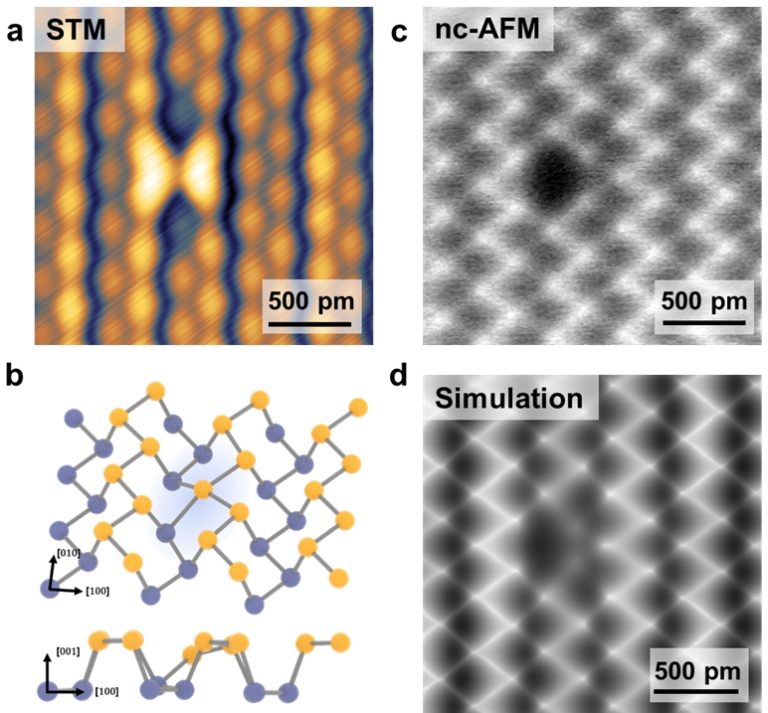
Physical characteristics of the self-passivated single vacancy (SV). (a) High resolution STM image of the self-passivated SV showing that it adopts a butterfly-shaped feature spanning over two of its nearest neighbours. (b) Atomic structure of the self-passivated SV with labelled crystallographic directions and the corresponding side-view (bottom panel). The yellow (violet) atoms indicate the phosphorus (P) atoms at the top (bottom) sublayers. (c) Atom-resolved nc-AFM image of the self-passivated SV, clearly showing that one P atom has been removed. (d) Simulated nc-AFM image of the self-passivated SV showing agreement with experimental results.
Prof Lu said, “In contrast to these conventional methods, the new passivation scheme reported may represent an ideal surface passivation strategy, which can selectively deactivate only the defect states without leaving a permanent crystal lattice change and degradation of the electronic performance. Our work opens up a new route for electronic self-passivation of defects, crucial for the further optimisation of the carrier mobility in BP and its analogs.”
Read the original article on National University of Singapore.