
Optical nano-imaging techniques find immense applications in nanotechnology for visualizing nanoscale defects in samples. However, it is challenging to image large micron-sized samples at nanoscale resolution owing to signal distortions resulting from unavoidable thermal and mechanical drifts of the system over time. Now, researchers from Japan have developed an ultrastable nano-imaging system that successfully detects unique nanoscale defects not observed in conventional nano-imaging in micron-scale tungsten disulfide samples, widening the technique’s scope to biological samples.
Raman spectroscopy, an optical microscopy technique, is a non-destructive chemical analysis technique that provides rich molecular fingerprint information about chemical structure, phase, crystallinity, and molecular interactions. The technique relies on the interaction of light with chemical bonds within a material. However, since light is a wave, optical microscopes are unable to resolve distances less than half the wavelength of the light incident on the sample. This is known as the “diffraction limit,” which prevents Raman spectroscopy and other optical microscopy techniques from reaching nanoscale resolutions.
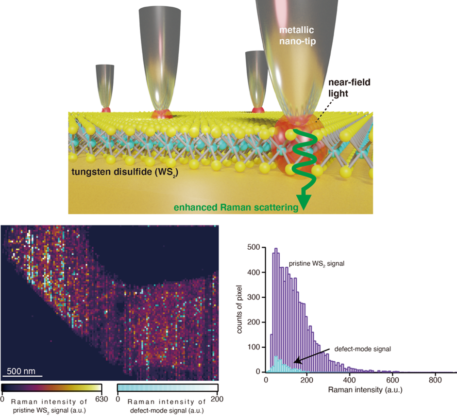
Figure 1. Long-duration tip-enhanced Raman imaging for defect analysis of large-sized WS2 layers. Conventional nanoscale imaging is usually difficult to perform for large, micron-scale samples owing to drifts caused by thermal effects and vibrations. Now, researchers from Japan address this issue with a newly developed imaging system that compensates for such drifts.
To improve the spatial resolution, another technique called “tip-enhanced Raman spectroscopy” (TERS) was invented, which can reach spatial resolutions below the diffraction limit. In TERS, a metallic nano-sized tip confines the light within a nano-sized volume just above the sample. The light interacts with the sample molecules on the surface and the imaging is performed by analyzing the scattered light.
TERS has been successfully used to analyze chemical compositions and surface defects in sample at nanoscale resolutions. However, during imaging, the nanotip tends to drift due to unavoidable thermal and vibrational fluctuations under ambient conditions, causing either the sample to be out-of-focus or misalignment between the nanotip and focal spot, or both. This causes considerable distortions in the scattered signals. To avoid this, TERS imaging needs to be completed within a time window of 30 minutes, a restriction that prevents imaging of any sample larger than 1 µm2 with nanoscale resolution.
In a new study published in Science Advances, a research team from Japan, led by Dr. Ryo Kato, a designated Assistant Professor at the Institute of Post-LED Photonics at Tokushima University, and Associate Professor Takayuki Umakoshi and Professor Prabhat Verma from Osaka University, has now developed, for the first time, a stable TERS system that is not limited to a short imaging time window. The team demonstrated its capability by successfully imaging nanoscale defects over a period of 6 hours in a micrometer-sized, two-dimensional (2D) tungsten disulfide (WS2) film – a material commonly used in optoelectronic devices. “Our new optical nano-imaging system enables characterization of defect analysis in large-sized WS2 layers at a high pixel resolution down to 10 nm without any significant loss of optical signal,” says Dr. Kato.
To compensate for the drifts over extended periods, the team developed a feedback system that tracks the displacement of the focused light source and readjusts the position of the focus plane accordingly. The focal position of the light source is tracked by measuring the displacement of a reflected laser guide beam directed into the microscope. The focus is then stabilized with a piezo-controlled objective scanner whenever the system senses a drift or a change in the focal position of the light source.
To stabilize the nanotip, the team designed a laser-scanning-assisted tip drift compensation system. In this case, galvano-scanners take images of the laser spot around the metallic nanotip just as it approaches the sample surface. This image appears as a bright spot and indicates the position of the nanotip. Once the measurement at a particular pixel has been carried out, the image of the laser spot around the nanotip is captured again. The laser spot is then moved to match the new position of the nanotip in this image. The process continues throughout the imaging process, ensuring the nanotip remains at a constant position.
By implementing these corrections, the team was able to image a 2D sheet of WS2 (Figure 1) with a scan area of 1 × 4 µm2. With a 12 times longer imaging time window than that of conventional imaging, they could detect unique defects missed in conventional TER imaging. They also showed that the defect density on a larger WS2 sample (comparable to device scales) was higher than that reported for smaller samples.
The study could open doors to precise, high-resolution imaging of not only optoelectronic devices but also biological samples. “Our new drift-compensated TERS microscopy could not only evaluate surface properties of device materials better but also allow us to study biological processes such as the mechanism underlying the development of diseases. This, in turn, could help develop novel clinical methods and therapies,” speculates Dr. Umakoshi. These are certainly some exciting possibilities to contemplate!
Read the original article on Tokushima University.