The quest for an ideal switching device for ultra-low power applications leads to an exploration of novel micro/nanoelectromechanical systems (M/NEMS) switches. This research has been driven by the superior performance of M/NEMS devices, such as ideally abrupt switching with zero off-state leakage, suitability for harsh and extreme environments, and very small footprints. The suspended element of the NEMS switch is electromechanically moved by the applied electric field to establish physical contact with the counterpart of the switch, and thereby the conducting channel is established.
However, an unacceptably high switching voltage of NEMS switches is the main obstacle to their practical use in low-power integrated circuits. In particular, sub-0.5 V switching voltage with a very small switch footprint, which is needed for ultra-low power circuits, has not yet been realized because of irreversible switching failures caused by surface adhesion. Moreover, once physical contact is created in NEMS switches, the switch contact area is increased, which leads to the domination of the surface attraction force over the mechanical restoring force; and as a result, permanent adhesion occurs.
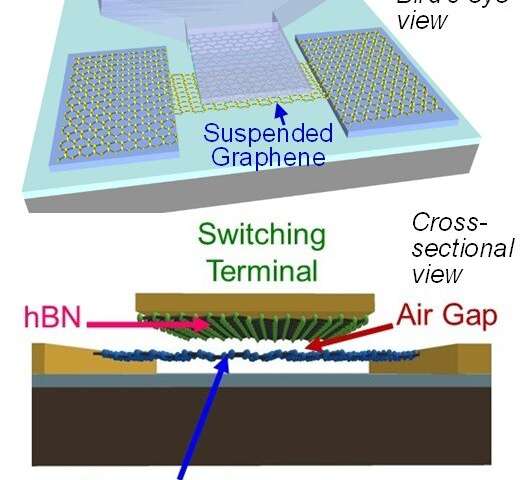
Figure 1 Schematic diagrams of the bird’s eye view (upper) and the cross-sectional view (lower) of the suspended graphene-hBN contact NEMS switch.
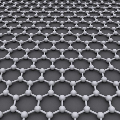
To succeed in creating a NEMS switch for ultra-low power applications, the material thickness has to be reduced and the switch contact adhesion in the ON state has to be overcome to reach the OFF state. The research team led by Dr. Manoharan Muruganathan (Former Senior Lecturer), and Professor Hiroshi Mizuta at the Japan Advanced Institute of Science and Technology (JAIST) proposed a graphene-based NEMS switch for this purpose. In the NEMS switch, the switching voltage is directly proportional to the suspended beam thickness, whereas the graphene monolayer is the thinnest material in the world today. Also, the graphene exhibits a cubic mechanical restoring force in the ON state, which is crucial to avoid stiction. Due to this unique characteristic, this research team pursued the graphene NEMS switch based on the doubly clamped suspended graphene beam with the hexagonal boron nitride (hBN) contact at the switching terminal (Fig. 1).
Graphene-to-hBN binding strength is low due to its van der Waals (vdW) bonding nature, which will overcome the stiction issue of NEMS switches, says researcher Dr. Ngoc Huynh Van of Technical University of Denmark. Based on the unique choice of materials and the NEMS switch design, they have demonstrated sub-0.5 V switching characteristics with more than 50,000 hot-switching cycles of operation. Moreover, these NEMS switches exhibit excellent switching characteristics, such as ~5 mV/dec switching slope, nearly-zero hysteresis, and >105 ON/OFF ratio, which meets the mainstream CMOS technology requirements.
These NEMS switches will play a vital role in various NEMS devices, sensors, NEM-CMOS hybrid integrated circuits, and ultralow-power applications.
Read the original article on Science X.