2023-03-07
Visited : 523
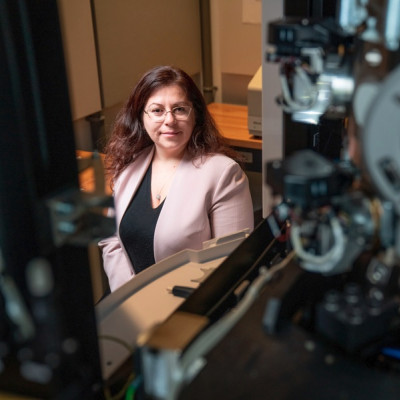
Materials scientist Anna Osherov helps researchers comprehend the nanoscale down to an atom using MIT.nano’s characterization tools.
Stroll past MIT.nano, the Institute’s center for nanoscience and engineering, and you can peer through large panes of glass at hundreds of tool sets ready to assist researchers in their scientific journey. Anyone who wants to take a closer look at what is happening at the nanoscale and beyond — even seeing individual atoms — will be welcomed by Anna Osherov, assistant director for Characterization.nano, helping researchers navigate a complex array of capabilities to apply the power of nanotechnology to new discoveries and next-generation technologies.
Osherov was among the first to join MIT.nano’s staff when it opened in 2018. Her purview encompasses instrumentation for metrology, imaging, and precise nanoscale analysis. This includes state-of-the-art technologies such as electron microscopy and spectroscopy, as well as instruments that measure mechanical, electrical, magnetic, and topographic properties. “Many of these tools are too expensive for individual labs to acquire and maintain, and too sensitive for use outside of highly-controlled environments,” says Osherov. “MIT.nano makes them more accessible and effective by grouping them in a central facility where they are open to the MIT community, as well as qualified external users from industry and academia.”
Most of the tools in Osherov’s domain are in the basement, protected from vibration and electromagnetic interference, or in cleanrooms and prototyping labs. In addition to the numerous instruments she oversees, the building contains complementary suites of fabrication equipment, administered by her staff counterpart Jorg Scholvin, for building and packaging novel materials and devices.
Strength of characterization
Characterization tool sets often support fundamental research, but they are also essential, Osherov says, as a “feedback mechanism” for refining the fabrication of everything from super-strong self-assembling polymers to cutting-edge solar cells. Making something in the lab is like cooking, she suggests: “You add a little bit of spices, adjust the time and temperature, and suddenly a very different product emerges from the same ingredients.” Much like chefs taste their food throughout the cooking process, characterization is used during fabrication to understand the effect of small adjustments on a product’s final properties.
Osherov and her colleagues assist dozens of users each month. Her exposure to many projects makes her well-positioned to be a cross-pollinator and offer advice. “Using equipment hands-on provides insight on the nuances of its capabilities and limitations that otherwise can be overlooked,” she observes. For example, knowing the characteristics of the surface on which the consecutive layers of new materials are deposited is crucial. “That's the canvas; it can dramatically affect further processing and the ultimate performance of the devices.”
Anticipating what researchers will need next, Osherov spearheads the program for onsite trial use of instruments. One example is the Raith VELION focused ion beam scanning electron microscope, which enables fabrication of 2D and 3D nanostructures and facilitates the study of electrical transport and surface modification. Osherov worked with several primary investigators to secure funding to purchase the microscope, which was initially installed as a long-term demo. “Validating that the instrument is useful for a diverse community at MIT and pursuing the grant to keep it on campus is a solid approach for shared equipment acquisition,” she says.
A broad view
Born in Crimea to a physician and musician, Osherov immigrated to Israel at age 12, following the collapse of the former Soviet Union. There, she graduated high school, served in the Israel Defense Forces, and pursued higher education.
As an undergraduate, Osherov joined the Perach-Israeli national volunteering program for social impact and focused on promoting female youth engagement in STEM. “It’s satisfying to see those kids becoming STEM advocates,” she says. At home, she talks of ions and atoms to her children (ages 3, 9, and 14), hoping to spark in them a lifelong excitement about science — or at the very least prevent a few actual kitchen disasters. “Not long ago I was explaining to my child how the microwave worked and why he shouldn’t put the thermos in it,” she laughs.
Osherov earned her materials science doctorate at Ben-Gurion University of the Negev studying mechanisms of heteroepitaxial growth in semiconductors. She was attracted to materials science because of its breadth and interdisciplinary perspective — as she puts it, “Everything around us is material.” Her studies and early career incorporated wide-ranging interests in physics and chemistry, in both basic and applied research, and in sectors including energy and health. Spending time in shared experimental facilities using state-of-the-art characterization tools was a big part of Osherov’s PhD experience, which has carried over to her current role.
She came to Massachusetts for a postdoc at Tufts University focused on solar cells and supercapacitors. She joined MIT in 2013 as a research scientist studying the correlation between structure, optoelectronic properties, and stability of perovskite solar devices, and as manager of the eni-MIT Solar Frontiers Shared Experimental Facilities. As Osherov balanced her own investigations with supporting the Solar Frontiers facility, she felt increasingly drawn to the latter role‚ making an impression on that center’s co-leader, Vladimir Bulović, now the director of MIT.nano.
“Anna was always diligently working on her own research while finding time to simultaneously support others,” says Bulović, the Fariborz Maseeh Professor in Emerging Technology. “As MIT.nano’s new research facilities started to be established, it was evident a strong leader was needed. Anna was our clear choice. Her passion for scientific exploration, understanding of the technical needs of the community, and demonstrated commitment to others made Anna the ideal candidate to shape, build, and lead MIT.nano’s characterization facility.”
Describing what it’s like to work at MIT.nano, Osherov uses the word “warmth.” She’s not referring to its labs’ carefully regulated temperature and humidity, of course, but to its welcoming social climate. “MIT.nano’s leadership assembled a strong team with complementary technical skills who are motivated to help so you don’t have to struggle to find your way,” she wants users to know. “We are here to search for solutions and address problems right alongside you.”
That’s true of the facility’s growing staff, and Osherov has observed the same helpfulness among researchers from different disciplines who share the space.
“There are a lot of transitional techniques that span across fields,” she says. “Some techniques that were used in the metallurgic industry decades ago can reemerge in biological fields or in 2D materials. We can learn from each other and reapply the power of well-established technologies toward new discoveries and new applications.”
“Often,” she adds, “just viewing things from a different angle gives a lot of new insight.”
Read the original article on Massachusetts Institute of Technology (MIT).