Nobel laureate Herbert KROEMER had famously observed that “the interface is the device”. When two-dimensional (2D) semiconductor materials are put in contact with metals, they form metal-semiconductor interfaces. These interfaces influence parameters such as contact resistance and play a critical role in the performance of the device. Even the nature of the charge carriers is largely determined by these interfaces. If electrons need a lower energy to cross the energy barrier at the interface, the polarity is “n-type”; if holes need a lower energy to cross the energy barrier at the interface, the polarity becomes “p-type”. Contact polarity is important for the design of device functionalities, such as p-n junctions.
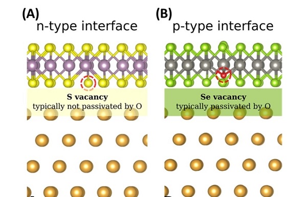
Figure A shows the atomic structure of molybdenum disulphide (MoS2) on gold metal. The sulphur (S) vacancies are typically not passivated by oxygen available in the environment and this results in a n-type interface. Figure B shows the atomic structure of tungsten diselenide (WSe2) on gold metal. The more reactive selenium (Se) vacancies are passivated by oxygen atoms (shown by the red dot). This turns it into a p-type interface.
A team of researchers led by Associate Professor QUEK Su Ying from the Department of Physics, NUS, used state-of-the-art calculations to study two common 2D semiconductor materials known as the transition metal dichalcogenides, MoS2 and WSe2, in contact with gold metal.
Prof Quek said, “Our calculations showed that both MoS2/gold and WSe2/gold contacts are p-type when there are no defects. These results were different from previous theoretical predictions. The crucial difference is that many-body exchange and correlation effects beyond a mean-field description are important to accurately predict the level alignment. When there is a chalcogen vacancy defect, the contacts become n-type in both cases. This is due to the additional energy levels in the band gap, which cause the energy levels of the metal to be “pinned”.”
Dr Keian NOORI, the lead author on this work, said, “Unlike MoS2, the chalcogen vacancy defects in WSe2 are more reactive. Under ambient conditions, oxygen available in the environment can react with these vacancies and remove the states in the band gap, so that the WSe2 material behaves like a pristine material with no defects, which is p-type, as far as contact polarity is concerned.”
Prof Quek added, “Although the chalcogen vacancy defects in MoS2 are less reactive, it is conceivable that experimental conditions can be arranged to allow the defects to be similarly “passivated” by oxygen or other species. This will then provide a route to enable more tunable control of the energy offset at the MoS2/metal contacts. As defects are often inevitable, knowing how to control their impact on key device properties will greatly help to optimise device performance.”
Read the original article on National University of Singapore (NUS).