
A novel class of two-dimensional (2D) nanomaterials based on organic-inorganic lead halide perovskites has recently been inaugurated to address the stability challenge in innovative optoelectronics in general and solar cells in particular. Their unprecedented emergence has pushed clean energies closer to the market. 2D perovskites are considered as a possible alternative to three-dimensional (3D) lead halide perovskites, which are commonly employed as the light-absorbing layer in the next-generation solar cells, to compensate for the short lifetime and stability of 3D counterparts and improve the levelized cost of electricity (LCOE).
This class of nanomaterials takes the general formula of (A)2(B)n−1PbnX3n+1, in which X and B stand for halides and cations, respectively, and A is a long-chain cation used as a spacer to slice the 3D frameworks into 2D ultrathin layers with nanometer thicknesses, which depend on the n integer.
The crystal lattice of these structures is schematically shown in Fig. 1. (HOOC(CH2)2NH3)2PbI4 and (C6H5(CH2)2NH3)2(CH3NH3)2Pb3I10 are examples of these compounds. Such nanomaterials are quantum-well structures containing the ultrathin slabs of perovskite, which are separated by the spacer layers. Their potential in light absorption is broadly comparable with that of silicon. The bulky spacers are intrinsically hydrophobe, and therefore enhance the film resistance against water molecules and moisture so that 5-ammonium valeric acid iodide (5-AVAI) can ensure one-year stability in photovoltaic devices.
This layered structure provides a considerable variation in conductivity along with perpendicular and parallel directions. Moreover, they can be used to improve the performance of LEDs by providing additional charge pathways within the devices. Their discovery has also opened a new window for the introduction of innovative electrical conduction in electronics. Additionally, 2D perovskites are proper candidates for triboelectric nanogenerators (TENG) to convert mechanical energy into electricity. Consequently, 2D perovskites come up with a promising insight into the production of efficient, stable nano-optoelectronics.
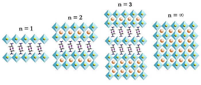
Figure 1. Schematic illustration of 2D perovskites [Chemsuschem 9 (2016) 2541].