2020-06-24
Visited : 5640
EPFL researchers have developed a high-precision technology that enables them to carve nanometric patterns into two-dimensional materials.
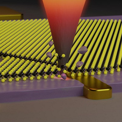
With their pioneering nanotechnology, EPFL researchers have achieved the impossible. They can now use heat to break the links between atoms with a miniature scalpel. “It’s extremely hard to structure 2D materials using conventional lithography, which often employs aggressive chemicals or accelerated, electrically charged particles, like electrons or ions, that can damage the material’s properties,” says Xia Liu, a researcher and postdoc in the School of Engineering’s Microsystems Laboratory. “Our technique, however, uses a localized heat and pressure ‘source’ to accurately cut into the 2D materials.”
“Our technology is similar to the art of paper-cutting, which is common in this region of Switzerland, but on a much smaller scale,” explains Ana Conde Rubio, co-author of the study. “We use heat to modify the substrate and make it more flexible and, in some cases, even turn it into a gas. We can then more easily carve into the 2D material.”
A sharp tip
Xia Liu, Samuel Howell, Ana Conde Rubio, Giovanni Boero and Jürgen Brugger used molybdenum ditelluride (MoTe2), a 2D material that’s similar to graphene. It’s less than a nanometer – or three layers of atoms – thick. The MoTe2 is placed on a polymer that reacts to changes in temperature. “When the polymer is exposed to heat, it sublimates, which means that it goes from a solid to a gaseous state,” explains Liu.
The researchers from the Institute of Microengineering used a new nanoscale structuring technique called thermal scanning probe lithography (t-SPL), which works in a similar way to an atomic force microscope. They heat a sharp nano-sized tip to more than 180°C, bring it into contact with the 2D material and apply a bit of force. This causes the polymer to sublimate. A thin layer of MoTe2 then breaks off without damaging the rest of the material.
Small and more efficient components
The researchers will be able to use this technology to carve extremely accurate patterns in 2D materials. “We use a computer-driven system to control the ultra-fast heating and cooling process and the position of the tip,” explains Samuel Howell, another co-author. “This enables us to make pre-defined indents to create, for instance, the nanoribbons that are used in nanoelectronic devices.”
But what’s so useful about working on such a small scale? “A lot of 2D materials are semi-conductors and can be integrated into electronic devices,” says Liu. “This generic technology will be very useful in nanoelectronics, nanophotonics and nanobiotechnology, as it will help to make electronic components smaller and more efficient.”
Enhancing the accuracy
The next phase of the research will focus on looking at a wider range of materials and finding combinations that will work in integrated nanosystems. Future activities will also revisit the design of the cantilever and nanotip for improved nano-cutting performance.
More broadly, the scientists in the Microsystems Laboratory are looking to develop a new generation of fabrication techniques for flexible microsystems. “Polymer-based microelectromechanical systems (MEMS) have a lot of potential electronic and biomedical applications,” explains Prof. Jürgen Brugger. “But we’re still in the early stages of developing techniques for designing functional polymers in 3D microsystems.” Brugger hopes to push the boundaries and find new materials and processes for MEMS by focusing on the stencil, the printing process, the directed self-assembly of nanomaterials, and localized thermal processing.
Read the original article on EPFL.