2020-09-15
Visited : 4809
Researchers from Stony Brook University in New York have discovered a way to make metal-metal composites and porous materials, within thin films, at nanometre scale
Scientists have found a way to form porous metal nanostructures in thin films. The findings could lead to improved biosensing devices in the future.
Medical Device Developments writer Natalie Healey speaks to Karen Chen-Wiegart, assistant professor in Stony Brook University’s Materials Science and Chemical Engineering Department, and a scientist at the National Synchrotron Light Source II, to explore the potential of the research.
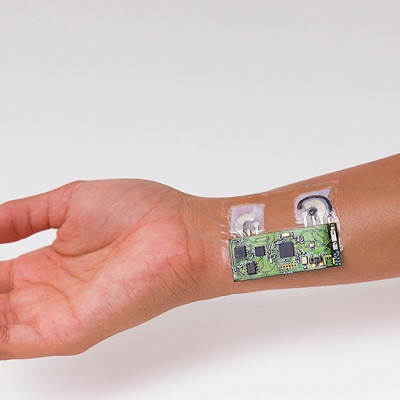
Biomedical sensors work by detecting medically relevant parameters such as pressure, temperature and certain molecules.
Such properties are vital for patient-monitoring, and more advanced diagnostic tests with greater sensitivity and specificity are constantly emerging.
It requires a combination of physics, biology and materials science to develop precision diagnostic devices that determine what is happening inside a patient.
There is much interest in how nanotechnology could be used to develop more sensitive tests that could ensure earlier diagnosis of various health conditions and hence improve patient outcomes.
While medical research isn’t Karen Chen-Wiegart’s area of expertise, her work could have important applications in biomedical sensing technology.
She is an assistant professor at Stony Brook University’s Materials Science and Chemical Engineering Department, and a scientist at the National Synchrotron Light Source II research facility – both of which are based in New York.
Chen-Wiegart and her students apply state-of-the-art X-ray imaging and spectroscopic techniques to study interconnected nanoscale materials.
Substances with this sponge-like morphology could be important for developing new biosensors and also have applications in energy storage and catalysis.
The team wanted to develop a way of making metal-metal composites and porous materials in thin films at nanometre scale.
Previous attempts had used a dealloying technique to create similar structures, but this had resulted in a size gradient, with a larger structure on one side of the sample, which would limit its applications.
“When we started this project, we were trying to address an issue in a fundamental aspect of dealloying,” explains Chen-Wiegart.
“It’s a process that involves forming a porous or bi-continuous structure, so you have an interconnected network of metallic structures.
“The process can be adjusted, so it gives you a really high surface area. And it’s because of this high surface area and the spontaneous process that it can be used to make a range of nanoporous materials.”
The aims of this project were to use dealloying to create thin-film structures, but instead of the conventional way of achieving these materials using liquid or molten metal, the team wanted to be able to do it in the solid state.
Although liquid metal dealloying (LMD) has been shown to successfully produce porous materials, the method tends to generate substances with larger ligament and pore sizes.
“Essentially, we wanted to simplify the dealloying process and to broaden the potential applications,” Chen-Wiegart says.
“And secondly, we wanted to be able to control this process and better understand the fundamental mechanism behind it.”
New process for creating porous nanostructures
The technique, called solid-state interfacial dealloying (SSID), uses heat to induce a self-organising process where the metals swap around to form a new structure.
The 3D interconnected metal-metal composites that form can be further treated to create thin films of porous metals with a high surface area.
The team demonstrated their technique by preparing magnesium, iron and nickel alloy films on silicon wafer substrates.
Samples were heated to 460ºC for 30 minutes and then rapidly cooled to room temperature – with the findings being published in peer-reviewed scientific journal Materials Horizons.
Turning up the heat gives the metals the energy to form a self-supported thermodynamically-stable structure.
The team’s work is the first time SSID has been used to create thin films of nanoporous materials that have a homogenous size distribution across the sample.
Usually scientists create porous metallic structures by putting metals into a leaching solution.
However, it was recently observed that the same process could occur using another metal to induce this spontaneous dealloying process.
“Imagine you’re breaking up a couple,” says Chen-Wiegart. “Another metal is essentially taking one of the elements so they rearrange and form the structure just as if you’d done the leaching in the acid.
“You’re just using the metal to attack the structure instead, but you have to choose the material properly so you can selectively remove an element from your initial structure.”
This had been achieved in both solid and molten metal states previously, but only with large materials.
The scientists wanted to do the process in nanofilm geometry, because that would open up the potential applications.
Chen-Wiegart says many uses are currently being explored, but the primary ones are in catalysis and energy storage.
“People are more familiar with nanoparticles,” says Chen-Wiegart. “But these are interconnected nanostructures that are self-supported.
“You end up with a sponge that can give you the benefit of nanoscale enhancement.”
The high surface area of the nanopores would improve reaction efficiency in photocatalysis, she says.
And the interconnected ligaments could provide electrically conductive pathways.
Nanoporous materials could be particularly useful in medical applications. These tiny sponge-like materials could enhance binding with specific enzymes and proteins to make more sensitive medical diagnostic devices in future.
“They engineer the surface and build a really high surface area,” points out Chen-Wiegart.
“So, it’s not just the pure materials, but you could potentially develop strategies to enhance sensitivity during the testing.
“Instead of having a flat surface, you have a convoluted porous surface. And by further tuning that surface you can create different types of biosensors that can selectively bind with different types of enzymes and so on.”
An enhanced focus
Chen-Wiegart reveals that one of the most exciting parts of the project was going to the National Synchrotron Light Source II to use two beamlines: the Hard X-ray Nanoprobe (HXN) and Beamline for Materials Measurement (BMM).
The facility enables scientists to study material properties at nanoscale resolution using X-ray imaging and high-resolution energy analysis.
Use of the facilities is free of charge for scientists working on open research, Chen-Wiegart explains.
The team used the scanning mode in a transmission electron microscope (TEM), moving the beam over the sample to generate 2D maps that would show the spatial distribution of the elements.
The same instrument was then used to obtain electron diffraction patterns to capture the 3D structure.
Then, a scanning electron microscope (SEM) was used to study surface morphology.
These techniques showed the scientists that an interconnected structure had indeed formed, but in order to ensure it was representative of the entire sample, the HXN beam was used as it can provide 3D information over a much larger region.
“With HXN, we can focus hard, or high-energy, X-rays to a very tiny spot of about 12nm,” says co-author Xiaojing Huang.
“The world-leading spatial resolution of hard X-ray microscopy at HXN is sufficient to see the sample’s smallest structures, which range in size from 20 to 30 nanometres.
“Though TEM provides higher resolution, the field of view is limited. With the X-ray microscope, we were able to observe the 3D element distributions within a bigger area so that we could confirm the homogeneity.”
“We used a range of techniques and combined their information to get a more comprehensive understanding,” adds Chen-Wiegart.
“We do elementary analysis not just in 2D, but in a three-dimensional fashion.
“So, you can see not just a 2D projection of your structure but you actually reconstruct the internal features and elemental distribution in three dimensions.
“Just imagine a CT scan. It’s a lot of effort, but once you get there it’s really cool.”
Now the researchers have demonstrated the feasibility of SSID for creating thin nanoporous films, they want to apply this approach to other metal systems and further explore the potential applications such as photocatalysis and biosensing.
“Right now, we’re working on titanium to form it into a pore structure,” Chen-Wiegart says. “And we want to really further understand some of the fundamentals.
“In the paper, we were able to get one of the first structures, but we want to be able to further control it and also push to start testing some of the properties for application.”
Read the original article on NS Medical Devices.