
In a study published in the New Journal of Physics, the researchers reported that firing intense laser pulses through a fiber-optic nanotip caused the tip to emit electrons, creating a fast “electron gun” that can be used to probe materials. The device allows researchers to quickly examine surfaces from any angle, which offers a huge advantage over less mobile existing techniques.
“It works on the principle of light activation, so light comes in and stimulates the electrons in the metal just in the right way for them to gain enough energy to come out,” said Ali Passian of ORNL’s Quantum Information Science group.
Electrons are an invaluable tool for getting an up-close look at surface features of materials. The subatomic particles, which have shorter wavelengths than photons — particles of light — can magnify objects at nanometer, or one billionth of a meter, resolution – exponentially higher than light magnification.
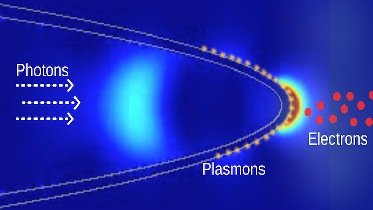
Light moves through a fiber and stimulates the metal electrons in nanotip into collective oscillations called surface plasmons, assisting electrons to leave the tip. This simple electron nano-gun can be made more versatile via different forms of material composition and structuring.
Since the mid-2000s, researchers have used sharp nanotips to emit electrons in tightly focused beams. The nanotips provide improved spatial and temporal resolution compared with other scanning electron microscopy techniques, helping researchers better track ongoing interactions at the nanoscale. In these techniques, electrons are emitted when photons excite the tips.
Before this study, however, nanotip emission methods have relied on external light stimulation. To generate electrons, researchers had to carefully align laser beams onto the apex of the nanotip.
“Previously, lasers had to track the tips, which is technologically a much harder thing to do,” said Herman Batelaan, a coauthor on the study who leads electron control research at the University of Nebraska. The difficulty of the task limited how quickly images could be taken and from what position.
But Passian had an idea for a different approach. By firing laser light through a flexible optical fiber to illuminate its tapered, metal-coated nanotip from within, he predicted that he could create a more easily maneuverable tool.
“The idea was that because this is simple and contained – the light propagates from the inside – you can probe different parts of the material at different heights and lateral positions,” Passian said.
To find out whether his idea was possible, Passian teamed up with Batelaan and then graduate student Sam Keramati at the University of Nebraska. The Nebraska team used a femtosecond laser to shoot ultrashort, intense pulses through an optical fiber and into a vacuum chamber. In the chamber, the light moved through a gold-coated fiber nanotip that had been fabricated at ORNL.
The team indeed observed controlled electron emission from the nanotip. Analyzing the data, they proposed that the mechanism enabling the emission is not a simple one, but rather includes a combination of factors.
One factor is that the shape and metal coating of the nanotip generates an electric field that helps push electrons out of the tip. Another factor is that this electric field at the nanotip’s apex can be enhanced by specific wavelengths of laser light.
“By tuning the femtosecond laser to the correct wavelength, which we call the surface plasmon resonance wavelength, we found that we got above threshold emission,” Keramati said. Surface plasmon resonance signifies a collective oscillation of the electrons at the surface of the metal. Above threshold emission occurs when electrons absorb enough energy from photons to be shot out with an initial kinetic energy.
To verify that the electrons were emitted due to light and not heat, the team studied the nanotips themselves. The tips sustained no damage during the experiment, indicating that the emission mechanism is indeed light driven.
An additional advantage of the new technique, they found, is that the fast-switching capacity of the laser source allows them to control electron emission at speeds faster than a nanosecond. This will give them better way to capture images at a fast rate. Such images can then be pieced together almost like a movie to track complex interactions on the nanoscale.
Turning down the power
Pleased with these initial findings, the team decided to test if they could achieve a similar outcome with a far less powerful continuous wave laser, the same type found in an everyday laser pointer. To compensate for the lack of laser power, they upped the voltage at the nanotip, creating an energy potential difference they believed could help expel electrons. To their surprise, it worked.
“To our knowledge this is the smallest laser intensity that has given rise to electron emission from nanotips,” Keramati, now a postdoctoral researcher, said of the results published in Applied Physics Letters.
“Now instead of having a powerful, extremely expensive laser, you can go with a $10 diode laser,” Batelaan noted.
Though continuous wave lasers lack the fast switching capabilities of more powerful femtosecond lasers, slow switching offers its own advantages; namely, the possibility to better control the duration and number of electrons emitted by nanotips.
The team demonstrated, in fact, that the control provided by slow switching enabled electron emission within the bounds necessary for a futuristic application called electron ghost imaging. Recently demonstrated light ghost imaging harnesses quantum properties of light to image sensitive samples, such as living biological cells, at very low exposure.
By bundling multiple fiber nanotips together, the team hopes to achieve electron ghost imaging on the nanoscale.
Read the original article on Oak Ridge National Laboratory.