2020-11-12
Visited : 2077
Blue phosphorus, an atomically thin synthetic semiconductor, becomes metallic as soon as it is converted into a double layer. This has been discovered by an interdisciplinary team led by Prof Thomas Heine from TU Dresden and Prof Gabriel Merino from the Mexican research institute Cinvestav Merida. The scientists are first to describe the possibility of constructing nanoscale, highly efficient transistors consisting of only one element. The results of these investigations were published as highlight article in the current issue of the journal "Physical Review Letters".
The scientists are first to describe the possibility of constructing nanoscale, highly efficient transistors consisting of only one element. The results of these investigations were published as highlight article in the current issue of the journal "Physical Review Letters".
The chemical element phosphorus is considered one of the most essential elements for life. Phosphorus compounds are deeply involved in the structure and function of organisms. Every human carries about one kilogram of it in the body. But even outside our bodies we are surrounded by phosphates and phosphonates every day: in our food, in detergents, fertilizers or in medicines.
Phosphorus occurs in several modifications that have extremely different properties. Under normal conditions, a distinction is made between white, purple, red and black phosphorus. In 2014, a team from the Michigan State University, USA, computationally predicted "blue phosphorus", which could be produced experimentally two years later.
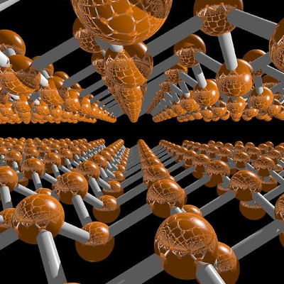
Blue phosphorus is a so-called two-dimensional (2D) material. Due to its single-layer honeycomb-like structure, it is reminiscent of what is probably the best known 2D material: graphene. Analogous to its famous forerunner, it was then also called blue phosphorene. This novel semiconductor material has since been investigated as an extremely promising candidate for optoelectronic devices.
The Dresden chemist Prof Thomas Heine, in cooperation with Mexican scientists, has now made a unique discovery: by applying a topological concept they identified computationally a remarkably stable two-layer buckled honeycomb structure of blue phosphorene by means of highly precise calculations on high-performance computers. This two-layered compound is extremely stable. As the scientists surprisingly discovered, it has metallic properties due to the very small distance between the two layers.
Like all components, these devices must be supplied with power, which usually enters the material via metal electrodes. At the metal-semiconductor interface, energy losses are inevitable, an effect known as the Schottky barrier. Blue phosphorus is semiconducting as a single layer, but predicted to be metallic as a double layer. Metallic 2D materials are very rare, and for the first time a pure elemental material has been discovered that exhibits a semiconductor-metal transition from the monolayer to the double layer. Thus, an electronic or optoelectronic component for use in transistors or photocells can be realized from only one chemical element. Since there is no interface between semiconductor and metal in these devices, the Schottky barrier is greatly reduced and a higher efficiency can be expected.
"Imagine you put two layers of paper on top of each other and suddenly the double sheet shines metallically like gold foil. This is exactly what we predict for blue phosphorene. This work underlines the importance of interdisciplinarity in basic research. Using a topological-mathematical model and theoretical chemistry, we were able to design a new material on the computer and predict its physical properties. Applications in the field of nano- and optoelectronics are expected," explains Prof Heine.
Read the original article on TU Dresden.