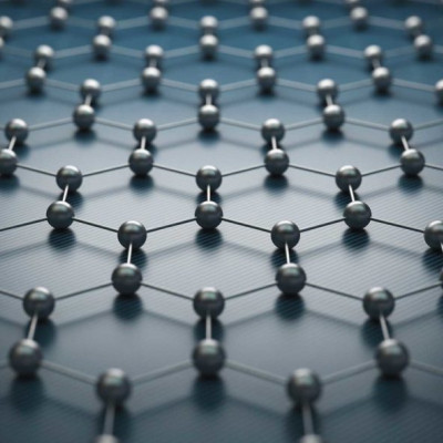
Graphene, an atomically thin carbon layer through which electrons can travel virtually unimpeded, has been extensively studied since its first successful isolation more than 15 years ago. Among its many unique properties is the ability to support highly confined electromagnetic waves coupled to oscillations of electronic charge—plasmon polaritons—that have potentially broad applications in nanotechnology, including biosensing, quantum information, and solar energy.
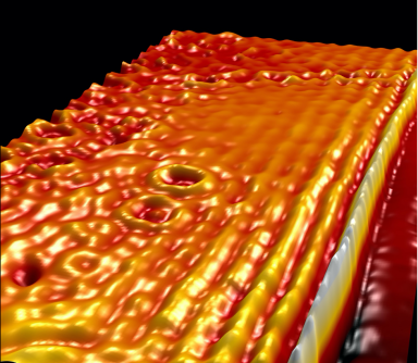
Massive work function-mediated charge transfer in graphene/a-RuCl3 heterostructures provides the necessary conditions for generating plasmon polaritons without electrostatic or chemical doping. The image depicts a characteristic infrared near-field image of such a heterostructure, revealing a host of plasmonic oscillations derived from substantial mutual doping of interfacial graphene/a-RuCl3 layers.
However, in order to support plasmon polaritons, graphene must be charged by applying a voltage to a nearby metal gate, which greatly increases the size and complexity of nanoscale devices. Columbia University researchers report that they have achieved plasmonically active graphene with record-high charge density without an external gate. They accomplished this by exploiting novel interlayer charge transfer with a two-dimensional electron-acceptor known as a-RuCl3. The study is available now online as an open access article and will appear in the December 9th issue of Nano Letters.
“This work allows us to use graphene as a plasmonic material without metal gates or voltage sources, making it possible to create stand-alone graphene plasmonic structures for the first time,” said co-PI James Hone, Wang Fong-Jen Professor of Mechanical Engineering at Columbia Engineering.
All materials possess a property known as a work function, which quantifies how tightly they can hold on to electrons. When two different materials are brought into contact, electrons will move from the material with the smaller work function to the material with the larger work function, causing the former to become positively charged and the latter to become negatively charged. This is the same phenomenon that generates static charge when you rub a balloon against your hair.
a-RuCl3 is unique among nanomaterials because it has an exceptionally high work function even when it is exfoliated down to a one- or few-atom-thick 2D layers. Knowing this, the Columbia researchers created atomic-scale stacks consisting of graphene on top of a-RuCl3. As expected, electrons were removed from the graphene, making it highly conductive and able to host plasmon polaritons—without the use on an external gate.
Using a-RuCl3 to charge graphene brings two main advantages over electrical gating. a-RuCl3 induces much greater charge than can be achieved with electrical gates, which are limited by breakdown of the insulating barrier with the graphene. In addition, the spacing between graphene and the underlying gate electrode blurs the boundary between charged and un-charged regions due to “electric field fringing.” This prevents realization of sharp charge features within the graphene and along the graphene edge necessary to manifest novel plasmonic phenomena. In contrast, at the edge of the a-RuCl3, the charge in the graphene drops to zero on nearly the atomic scale.
“One of our major achievements in this work is attaining charge densities in graphene roughly 10 times larger than the limits imposed by dielectric breakdown in a standard gated device,” said the study’s lead PI Dmitri Basov, professor of physics. “Moreover, since the a-RuCl3—the source of electronic charge—is in direct contact with graphene, the boundaries between the charged and uncharged regions in the graphene are razor-sharp. This allows us to observe mirror-like plasmon reflection from these edges and to create historically elusive one-dimensional edge plasmons that propagate along the graphene edge.” The team also observed sharp boundaries at “nano-bubbles,” where contaminants trapped between the two layers disrupt charge transfer.
“We were very excited to see how abruptly the graphene charge density can change in these devices,” said Daniel Rizzo, a postdoctoral research scientist with Basov and the lead author on the paper. “Our work is a proof-of-concept for nanometer charge control that was previously the realm of fantasy.”
The work was carried out in the Energy and Frontier Research Center on Programmable Quantum Materials funded by the United States Department of Energy and led by Basov. The research project used shared facilities operated by the Columbia Nano Initiative.
The researchers are now pursuing routes to use etched a-RuCl3 as a platform for generating custom nanoscale charge patterns in graphene to precisely tune the plasmonic behavior according to various practical applications. They also hope to demonstrate that a-RuCl3 can be interfaced with a wide range of 2D materials to access novel material behaviors that require the exceptionally high charge density imparted by interlayer charge transfer demonstrated in their manuscript.
Hone noted, “When our interlayer charge transfer technique is combined with existing procedures for patterning 2D substrates, we can easily generate tailor-made nanoscale charge patterns in graphene. This opens up a wealth of new opportunities for new electronic and optical devices.”
Read the original article on Newswise.