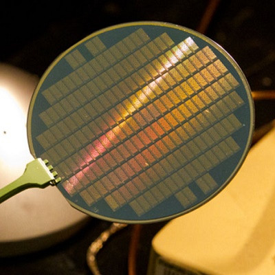
Carbon nanotube devices are getting closer to silicon’s abilities thanks to a series of developments, the latest of which was revealed at the IEEE Electron Devices Meeting (IEDM). Engineers from Taiwan Semiconductor Manufacturing Company (TSMC), University of California San Diego, and Stanford University explained a new fabrication process that leads to better control of carbon nanotube transistors.
Such control is crucial to ensuring that transistors, which act as switches in logic circuits, turn fully off when they are meant to. Interest in carbon nanotube transistors has accelerated recently, because they can potentially be shrunk down further than silicon transistors can and offer a way to produce stacked layers of circuitry much more easily than can be done in silicon.

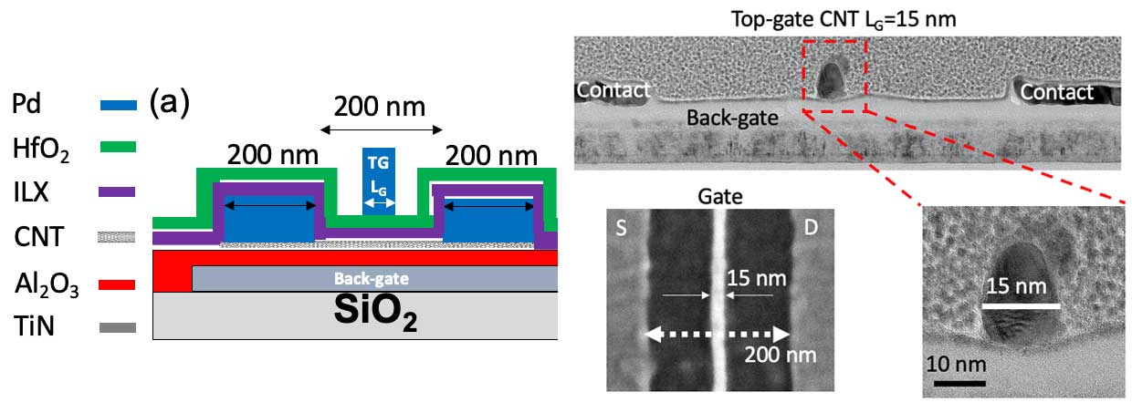
Heart of a Nanotube Transistor: Researchers sought better control of control of carbon nanotube transistors by using a thinner insulator between the nanotube [faint circle, center] and the transistor gate [top, black].
The team invented a process for producing a better gate dielectric. That’s the layer of insulation between the gate electrode and the transistor channel region. In operation, voltage at the gate sets up an electric field in the channel region that cuts off the flow of current. As silicon transistors were scaled down over the decades, however, that layer of insulation, which was made of silicon dioxide, had to become thinner and thinner in order to control the current using less voltage, reducing energy consumption. Eventually, the insulation barrier was so thin that charge could actually tunnel through it, leaking current and wasting energy.
A little more than a decade ago, the silicon semiconductor industry solved this problem by switching to a new dielectric material, hafnium dioxide. This material has a high dielectric constant (high-k) compared to the silicon dioxide used previously, meaning that a relatively thick layer of high-k dielectric is electrically equivalent to a much thinner layer of silicon oxide.
Carbon nanotube transistors also use HfO2 gate dielectrics. The problem with carbon nanotubes is that they don’t allow the formation of a dielectric in the thin layers needed to control scaled-down devices.
The method that deposits high-k dielectrics is called atomic-layer deposition. As the name indicates, it builds materials one atomic layer at a time. However, it needs somewhere to start. In silicon, that’s the atom-thin layer of oxide that naturally forms at the surface.
Carbon nanotubes offer no such foothold for the deposition to begin. They don’t naturally form oxide layers—carbon dioxide and carbon monoxide are gases, after all. And any defects in the nanotube that would lead to the kind of “dangling bonds” needed would limit its ability to conduct current.
Until now, growing a thin layer of the high-k dielectric hafnium dioxide atop a carbon nanotube was impossible. Researchers are Stanford and TSMC solved the problem by adding an intermediate-k dielectric between them.
“Forming high-k dielectrics has always been a big problem,” says H.-S. Philip Wong, the TSMC chief scientist and Stanford University professor who led the work. You have to “basically, dump a much thicker oxide on top of the nanotube” than you’d want in a scaled-down transistor. To see why this is a problem, Wong suggests, imagine the action of the gate voltage as trying to stop water flowing through a garden hose by stepping on it with your foot. If you put a stack of pillows—analogous to a thick gate oxide—between your foot and the hose, it becomes much harder.
Matthias Passlack at TSMC and Andrew Kummel at UCSD came up with a solution by combining atomic layer deposition of HfO2 with a new method of depositing an intermediate-dielectric-constant material, aluminum oxide. The Al2O3 is laid down using a process invented at UCSD called nanofog. Like water vapor condenses to form fog, the Al2O3 condenses into clusters that coat the nanotube surface. The atomic-layer deposition of HfO2 can then begin using this interfacial dielectric as a foothold.
The combined electrical characteristics of the two dielectrics allowed the team to build a device with a gate dielectric that was less than 4 nanometers thick beneath a gate that was just 15 nanometers across. The resulting device has similar on/off current ratio characteristics to those of silicon CMOS devices, and simulations indicate that even smaller devices with thinner gate dielectrics will work as well.
But there’s much more to be done before carbon nanotube devices can match silicon transistors. Several of the issues have been solved individually but have not yet been combined into a single device. For example, the single nanotube in Wong’s device limits how much current the transistor can drive. Getting multiple, identical, nanotubes aligned perfectly has been a challenge, says Wong. Researchers in the laboratory of Lian-Mao Peng at Peking University, in Beijing, recently managed to get 250 carbon nanotubes lined up per micrometer, suggesting a solution may soon be in-hand.
Another issue is the resistance between the device’s metal electrodes and the carbon nanotubes, especially when those contacts are scaled down to near the size used in advanced silicon chips today. Last year, one of Wong’s students, Greg Pitner (now a TSMC researcher and the lead author of the IEDM research), reported a way to bring that resistance for one type of contact (p-type) to within a factor of two of the theoretical limit for contacts just 10 nanometer across. However, n-type contacts to carbon nanotubes have not yet reached similar levels of performance, and you need both types for CMOS logic.
Finally, the carbon nanotubes need to be doped to increase the number of charge carriers on either side of the gate. Such doping is done in silicon by replacing some of the atoms in the crystal lattice with other elements. That won’t work in a carbon nanotube, because it would destroy the structure’s electronic abilities. Instead, carbon nanotube transistors use what’s called electrostatic doping. Here the composition of the dielectric layer is deliberately manipulated to donate electrons to the nanotube or to draw them out. Wong says that a former student, Rebecca Park, got good results using molybdenum oxide in this layer.
“We’re very excited, because we’re knocking down all these pieces one by one,” he says. “The next step is to put it all together… If we can combine all that, we’ll beat silicon.”
Read the original article on IEEE Spectrum.