
The logic circuits behind just about every digital device today rely on a pairing of two types of transistors—NMOS and PMOS. The same voltage signal that turns one of them on turns the other off. Putting them together means that electricity should flow only when a bit changes, greatly cutting down on power consumption. These pairs have sat beside each other for decades, but if circuits are to continue shrinking they’re going to have to get closer still.
This week, at the IEEE International Electron Devices Meeting (IEDM), Intel showed a different way: stacking the pairs so that one is atop the other. The scheme effectively cut the footprint of a simple CMOS circuit in half, meaning a potential doubling of transistor density on future ICs.
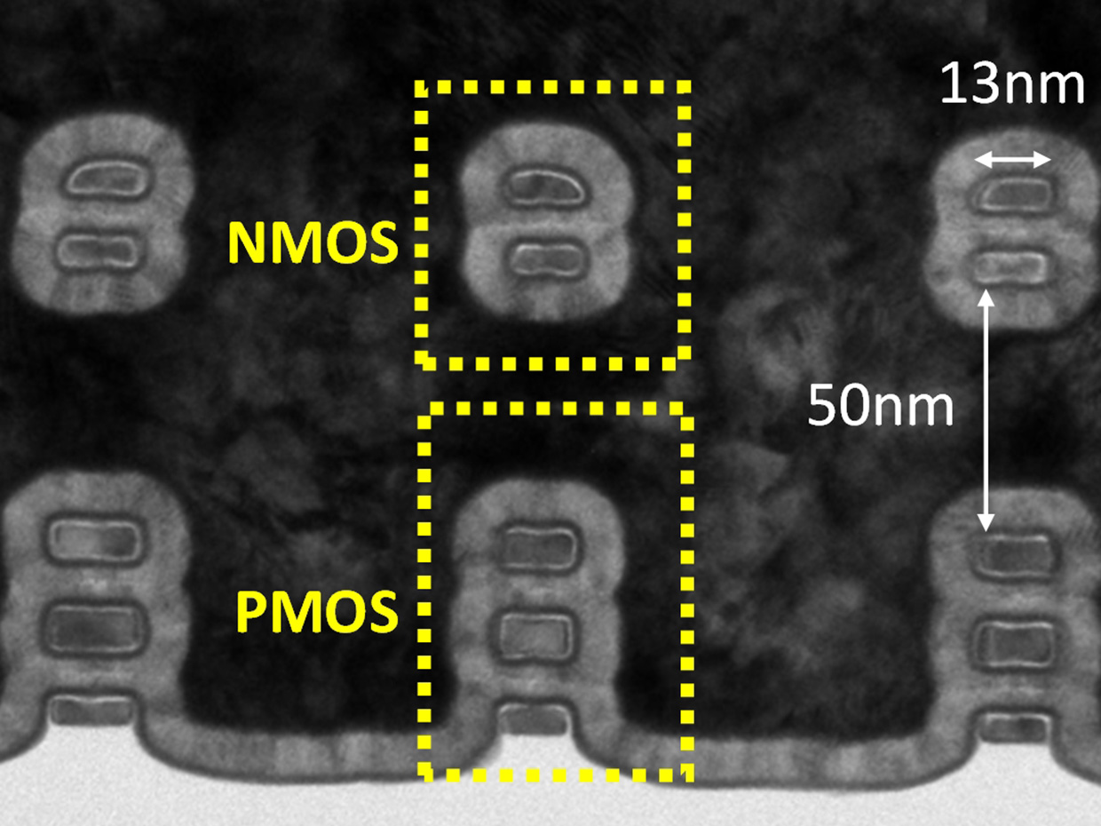
NMOS and PMOS devices usually sit side-by-side on chips. Intel has found a way to build them atop one another, compressing circuit sizes.
The scheme starts by using what’s widely agreed to be the next generation transistor structure, called variously nanosheet, nanoribbon, nanowire, or gate-all-around device depending on who’s involved. Instead of the main part of the transistor consisting of a vertical fin of silicon as it does today, the nanosheet’s channel region consists of multiple, horizontal, nanometers-thin sheets stacked atop one another.
Intel engineers used these devices to build the simplest CMOS logic circuit, an inverter. It requires two transistors, two connections to power, one input interconnect, and one output. Even when the transistors sit side-by-side, as they do today, the arrangement is very compact. But by stacking the transistors and adjusting the interconnects, the inverter’s area was cut in half.
CMOS devices have evolved from planar to FinFET. They will soon move to nanosheet. Shrinking circuits further will require stacking NMOS and PMOS devices.
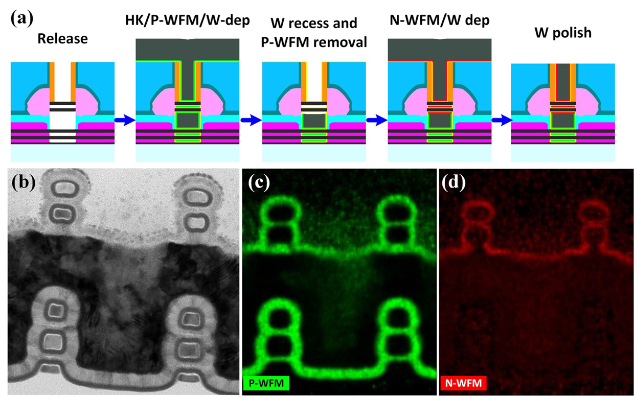
Intel’s recipe for building stacked nanosheets is called a self-aligned process because it builds both devices in essentially the same step. That’s important because adding a second step—say, by building them on separate wafers and then bonding the wafers together—could lead to misalignments that would destroy any potential circuits.
At its heart, the process is a modification of the steps involved in making nanosheet transistors. It starts with repeated layers of silicon and silicon germanium. This is then carved into a tall narrow fin, and the silicon germanium is etched away to leave a suspended set of silicon nanosheets. Ordinarily, all the nanosheets would go to form a single transistor. But here, the top two nanosheets are connected to phosphorous-doped silicon with the aim of forming an NMOS device, and the bottom ones to boron-doped silicon germanium to yield PMOS.
The full “integration flow” is, of course, more complicated, but Intel researchers worked hard to keep it as simple as possible, says Robert Chau, Intel senior fellow and director of components research. “Integration flow cannot be too complicated, because that will affect the practicality of making chips with stacked CMOS. This is a very practical flow with respectable results.”
“Once we get the hang of it, the next step will be to go after performance,” he says. That will likely involve improving the PMOS devices, which right now lag behind the NMOS in their ability to drive current. The answer to that problem is likely the introduction of “strain” to the transistor channel, says Chau.
The idea is to distort the silicon crystal’s lattice in such a way that charge carriers (holes in this case) flit through faster. Intel introduced strain into its devices back in 2002. In separate research at IEDM, Intel showed a method of producing both compressive strain and tensile strain in nanoribbon transistors.
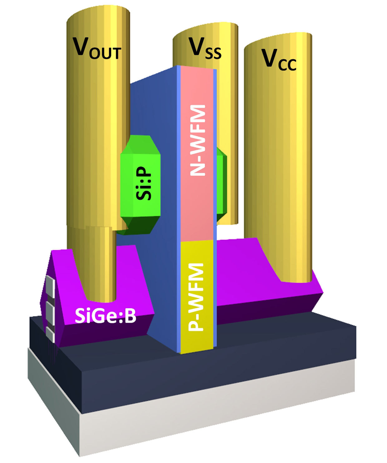
The inverter consists of two transistors on top of one another with some parts and interconnects in common.
Other research organizations are also pursuing stacked nanosheets designs, though they are sometimes called complementary FETs, or CFETs. The Belgian research organization Imec pioneered the CFET concept and reported constructing them at IEEE VLSI Symposia last June. However, the Imec components were not made completely from nanosheet transistors. Instead, the bottom layer consisted of a FinFET and the top was a single nanosheet.
Researchers in Taiwan reported the production of a CFET structure having a single nanosheet each for the PMOS and NMOS. In contrast, Intel’s circuit had a two-nanosheet NMOS atop a three-nanosheet PMOS, which is closer to what devices are likely to look like by the time stacking becomes necessary.
Read the original article on IEEE Spectrum.