2021-03-10
Visited : 1865
On March 3rd, the Artificial-intelligence Nano-photonic team led by academician Min GU published a high-level paper entitled “Nanoprinted high-neuron-density optical linear perceptrons performing near-infrared inference on a CMOS chip” in Light: Science and applications, making new findings in all-optical holographic nanostructure.
General introduction of the research: Intelligent holographic nanostructures on CMOS sensors for energy-efficient AI security schemes
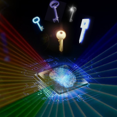
Today, machine learning permeates our everyday life, with millions of users every day unlocking their phones through facial recognition or passing through AI-enabled automated security checks at airports and train stations. These tasks are possible thanks to sensors that collect optical information to feed it to a neural network in a computer. Imagine to empower the sensors in the devices you use every day to perform artificial intelligence functions without a computer - as simply as putting glasses on them.
The integrated holographic perceptrons developed by a research team at University of Shanghai for Science and Technology led by Professor Min Gu, a foreign member of the Chinese Academy of Engineering, can make that a reality. They realized an AI optical circuit, with a neural density equal to 1/400 of human brain. The circuit is trained to process information through unpowered all-optical inference at the speed of light with a computational power more than ten orders of magnitude larger than electronic processors. In future, its neural density is expected to be 10 times that of human brain.
How it works
Traditionally, visual information is translated into electronic information, which is then processed by energy-hungry hardware. The technology Professor Gu’s team developed allows to skip this translation step, and process the optical information directly and without using any power.
Elena Goi, the first author of the published paper and a key member of Prof Gu’s team, said that the processing of optical information is enabled by state-of-the-art nanofabrication.
“By employing high-precision 3D nanofabrication technology, we are able to add AI optical elements to industry-standard imaging sensors. This is comparable to putting tailored, task-specific smart glasses on the imaging sensors, which process the incoming optical information before it is even detected.”
Impact
Using a state-of-the-art laser 3D-nanoprinting technology, the researchers fabricate optical perceptrons with a neuron density of over 500 million neurons per square centimetre. The nanoscale feature size of these smart optical elements pushes the upper limit for the computational power for the nanoprinted decryptors lies at 400 ExaFLOPS (1018 FLOPS, floating operations per second), an increase in the operations per second of five orders of magnitude compared with integrated photonic hardware.
By printing the perceptrons directly on CMOS imaging chips, Goi said, it is possible to realise AI optical circuits, which not only outperform current optical methods, but show the potential for application in a wide range of fields from security check, medical diagnostics, automatic driving, satellite image processing, etc.
According to Professor Gu, this technology will enable a whole new family of energy-efficient AI-enabled edge devices for processing optical information. This is of particular importance for applications where energy consumption is critical or data connectivity is limited, for example smart sensing devices in remote areas or smart sensors for long term deployment.
Read the original article on University of Shanghai for Science and Technology.