Since the early 2010s, ultrafast probing of materials at atomic-level resolution has been enabled by terahertz scanning tunneling microscopes (THz-STM). But these devices can't detect the dissipation of energy that happens during events such as when photons are emitted via recombination process of an electron-hole pair in a light emitting diode (LED). However, a new technique allows the tracking of just such energy dynamics alongside THz-STM, opening up new avenues of investigation for nanoscale science and technology.
Researchers in Japan have developed a microscopy technique that combines the ability to manipulate the motion of electrons on a femtosecond timescale and to detect a photon at sub-nanometer resolution. The new method offers a new platform for scientists to conduct experiments involving sensing and control of quantum systems, opening new doors for nanoscale science and the development of nanotechnologies.
The team, consists of scientists at Yokohama National University and RIKEN, published details of their technique in the journal ACS Photonics on January 27th.

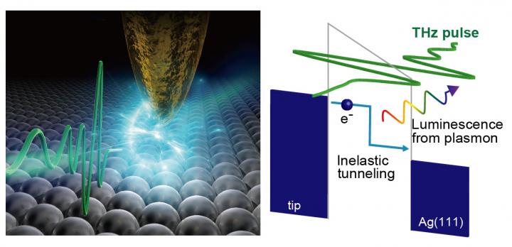
Basic concept of THz-field-driven scanning tunneling luminescence (THz-STL) spectroscopy. Luminescence from a localized plasmon can be induced by THz-field-driven inelastically tunneled electrons.
The scanning tunneling microscope (STM) was developed in 1981 as an instrument that produces images of surfaces at the atomic level. The technique depends upon the phenomenon of quantum tunneling, in which a particle "tunnels" through an otherwise impenetrable barrier. The surface that is being investigated by the microscope is sensed by a very fine and sharp conducting tip. When the tip approaches the surface, a voltage applied across the tip and the surface allows electrons to tunnel through the vacuum between them. The current produced by this tunneling in turn provides information about the object that can then be translated into a visual image.
STM took a big leap forward in the early 2010s with the THz-STM technique, which uses an ultrafast electric-field pulse at the scanning probe tip of an STM to manipulate electrons at a timescale of under a picosecond (a trillionth of a second).
This is great for ultrafast probing of materials at atomic-level resolution, but can't detect the dissipation of energy that happens during quantum conversions. This includes, for example, electron-photon conversions, which is what happens when an injection of electron, or hole, hits a LED, knocking loose exactly one photon inside the LED semiconductor material. It would be very useful to combine the ultrafast atomic-level resolution of STM with being able to track such dynamics of diffusion of energy.
A technology that can indeed track such dynamics, called scanning tunneling luminescence spectroscopy (STL), measures photons converted by tunneling electrons and has been developed in parallel to THz-STM. STL offers abundant information on photon energy, intensity, polarization and the efficiency of its emission, triggered by electron tunneling.
"But THz-STM and STL had never been combined before in a single set-up," said Jun Takeda of Yokohama National University, who co-led the study. "So we put the two techniques together."
A lens was placed in such a way as to focus THz pulses onto the tip of the STM. Photons produced from these pulses were then collected using a second lens and directed to a photon detector, allowing the desired investigation of the energy dynamics of quantum conversions that occur during STM ultrafast probing of materials at the atomic level.
This revealed an ultrafast excitation of plasmons (surface electrons) at extremely high voltage.
"This excitation in turn could provide a unique new platform for experimentation and exploration of light-matter interactions in a 'plasmonic nanocavity', says Ikufumi Katayama, who also co-led the study. Plasmonic nanocavity is a nanometer-scale structure for trapping light but that would involve these surface electrons.
The nanocavity method should allow investigation of energy dynamics resulting from electron tunneling in semiconductors, and in other molecular systems at the timescale of even a femtosecond--a quadrillionth of a second, or the amount of time it typically takes for molecular dynamics, the physical movement of individual atoms or molecules, to occur. This should allow greater sensing and control of quantum systems, providing novel insights and advances in nanoscale technology and science.
Read the original article on Scienmag.
