
Silicene, which is regarded as the silicon analogue of graphene, is a two-dimensional allotrope of silicon. In its normal state, a bulk silicon is a semiconductor with a diamond crystal type structure. As it thins down to one or several layers, its properties change dramatically. However, it has not yet been possible to study the change in the electronic properties of 2D materials at high pressure.
Scientists from Russia, Italy, the United States, and Belgium have developed a theoretical research method relying on quantum chemistry to study the electronic properties of 2D materials under pressure using silicene as an example. In contrast to carbon, which is stable in both 3D and 2D states, silicene is metastable and easy to interact with the environment. The paper was published in the ACS Nano journal.
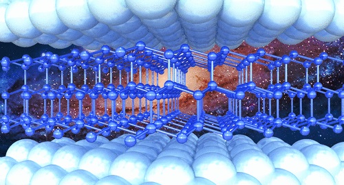
Modeling the behavior of 2D materials under pressure.
“Silicon is a semiconductor in its bulk state and a metal in the 2D state. The properties of monolayer and multilayered silicene are extensively studied theoretically. Silicene is corrugated rather than flat due to the interactions between the neighboring silicon atoms. An increase in pressure should flatten silicene and change its properties, but this effect cannot yet been investigated experimentally,” explains Skoltech research scientist Christian Tantardini.
In most cases, experimental tools used to apply pressure to the material along the axis normal to its plane simultaneously produce compression in the in-plane directions of 2D material. Thus, the resulting measurements would hardly be accurate, so right now modelling appears to be the only plausible approach.
“In our case, a new theoretical approach was the only solution. As pressure is applied only along one direction, we simulate the compression of our material and try to figure out what are the reason of the changes in the electronic structure, arrangement of silicon atoms and their hybridization under different pressures, and why the layers flatten,” Skoltech Senior Research Scientist Alexander Kvashnin comments.
Accurate prediction of the behavior of silicene or other 2D materials under pressure would make silicene a promising candidate for pressure sensors. When placed inside the sensor, silicene could help determine pressure based on the material’s response to compression. This kind of sensors could be used, for instance, in drilling rigs with a high requirement for pressure control to increase the drilling force without damaging the equipment.
“We used silicene in our modelling study to test the method which could also work for other 2D materials, including more stable ones that are already manufactured and used extensively, at zero pressure” says Xavier Gonze, a visiting professor at Skoltech and a professor at the Université catholique de Louvain (UCLouvain) in Belgium.
Read the original article on The Skolkovo Institute of Science and Technology (Skoltech).