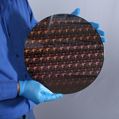
The company said the 2nm manufacturing process is the world's first and it allows 50 billion transistors to be monolithicially integrated in a "fingernail-sized" chip. This would achieve a world leading semiconductor manufacturing process density of 333 million transistors per square millimeter (if a fingernail measures 150 square millimeters).
The work was done at IBM's research lab at the Albany Nanotech Complex in Albany, NY.
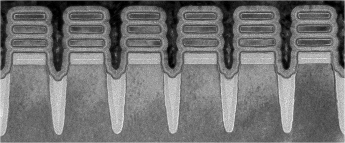
Cross section of IBM 2nm silicon manufacturing process.
IBM is no longer a volume manufacturer of chips and relies on foundry suppliers to produce its chips. IBM paid Globalfoundries $1.5 billion in 2015 to take over the remains of its chip manufacturing business and now relies on Samsung to make its most advanced processors (see IBM's 7nm Power10 processor is made by Samsung).
No details have been provided of the chip produced but such test chips are usually based on SRAM arrays and logic. But in the long term the process is likely intended as platform for IBM processors but has been declared as also being suitable for 6G, AI and smartphone applications.
The process includes three gate-all-around (GAA) nanosheet channels in each fin. Extreme ultraviolet (EUV) processing is necessary to define the small dimensions in the process but it allows nanosheet widths of between 15nm and 70nm. In an echo of IBM's earlier work on silicon-on-insulator (SOI) the process includes a bottom dielectric isolation to enable 12nm gate length. IBM has developed an inner spacer dry process to provide precise gate dimension control. The process supports multiple threshold voltages for both SoC and high-performance computing applications.
It is not clear how much strain engineering or whether novel materials were used in the transistor channels.
IBM reckons that the processor systems implemented in the 2nm manufacturing process are projected to achieve 45 percent higher top performance than in the 7nm process or could consume 75 percent less energy than those doing the same work in 7nm.
Next: Something for Intel? But years away?
It is notable that Intel announced last month that as part of its re-entry to the foundry business it would team up with IBM to research process technology and packaging for future chips. So IBM's proposed 2nm manufacturing process could represent part of Intel's path back to chip manufacturing excellence.
Intel, once the unrivalled leader in chip manufacturing technology, has struggled to bring up its 10nm and 7nm manufacturing processes over the last decade and now lags behind TSMC and Samsung who are at 5nm.
But it should also be noted that IBM has been making slow progress.
IBM's latest announcement comes four years after its presented its 5nm nanosheet process as part of a research alliance with Globalfoundries and Samsung. And six years after it announced the production of a prototype 20 billion transistor chip on a 7nm process. While IBM announced details of the Power10 processor in 2020 it has said that IBM computers based on the Power10 on 7nm will come to market in the second half of this year.
At that rate the IBM 2nm manufacturing process could take until 2027 to start being used in products. By contrast TSMC is expected to start production of its 3nm gate-all-around GAA process in 2022 with the 2nm GAA in R&D.
Read the original article on eeNews Analog.