A UNSW study out this month shows that the resulting high-mobility components are ideal candidates for high-frequency, ultra-small electronic devices, quantum dots, and for qubit applications in quantum computing.
Smaller means faster, but also noisier
Making computers faster requires ever-smaller transistors, with these electronic components now only a handful of nanometres in size. (There are around 12 billion transistors in the postage-stamp sized central chip of modern smartphones.)
However, in even smaller devices, the channel that the electrons flow through has to be very close to the interface between the semiconductor and the metallic gate used to turn the transistor on and off. Unavoidable surface oxidation and other surface contaminants cause unwanted scattering of electrons flowing through the channel, and also lead to instabilities and noise that are particularly problematic for quantum devices.
“In the new work we create transistors in which an ultra-thin metal gate is grown as part of the semiconductor crystal, preventing problems associated with oxidation of the semiconductor surface,” says lead author Yonatan Ashlea Alava.
“We have demonstrated that this new design dramatically reduces unwanted effects from surface imperfections, and show that nanoscale quantum point contacts exhibit significantly lower noise than devices fabricated using conventional approaches,” says Yonatan, who is a FLEET PhD student.
“This new all single-crystal design will be ideal for making ultra-small electronic devices, quantum dots, and for qubit applications,” comments group leader Prof Alex Hamilton at UNSW.
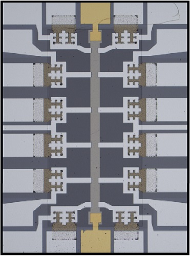
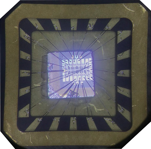
Close-up: the heterostructure device being constructed and studied at UNSW.
The challenge: electron scattering limits high-frequency components
Semiconductor devices are a staple of modern-day electronics. Field-effect transistors (FETs) are one of the building blocks of consumer electronics, computers and telecommunication devices.
High electron-mobility transistors (HEMTs) are field-effect transistors that combine two semiconductors with different bandgap (ie, they are ‘heterostructures’) and are widely used for high-power, high-frequency applications such as cell phones, radar, radio and satellite communications.
These devices are optimised to have high conductivity (in comparison to conventional MOSFET devices) to provide lower device noise and enable higher frequency operations. Improving electron conduction within these devices should directly improve device performance in critical applications.
The quest to make increasingly smaller electronic devices demands the conducting channel in HEMTs to be in close proximity to the surface of the device. The challenging part, which has troubled many researchers over the years, has its roots in simple electron transport theory:
When electrons travel in solids, the electrostatic force due to unavoidable impurities/charge in the environment causes the electron trajectory to deviate from the original path: the so-called ‘electron scattering’ process. The more scattering events, the more difficult it is for electrons to travel in the solid, and thus the lower the conductivity.
The surface of semiconductors often has high levels of unwanted charge trapped by the unsatisfied chemical bonds– or ‘dangling’ bonds – of the surface atoms. This surface charge causes scattering of electrons in the channel and reduces the device conductivity. As a consequence, when the conducting channel is brought close to the surface, the performance/conductivity of the HEMT plunges rapidly.
Additionally, surface charge creates local potential fluctuations which, apart from lowering the conductivity, result in charge-noise in sensitive devices such as quantum point contacts and quantum dots.
Electrical characterisation of the new heterostructure device demonstrated greatly reduced surface-charge scattering, and a significant improvement in conductivity.
The solution: growing the switching gate first reduces scattering
Collaborating with wafer growers at Cambridge University, the team at UNSW Sydney showed that the problem associated with surface charge can be eliminated by growing an epitaxial aluminium gate before removing the wafer from the growth chamber.
“We confirmed the performance improvement via characterisation measurements in the lab at UNSW,” says co-author Dr Daisy Wang.
The team compared shallow HEMTs fabricated on two wafers with nearly-identical structures and growth conditions – one with an epitaxial aluminium gate, and a second with an ex-situ metal gate deposited on an aluminium oxide dielectric.
They characterised the devices using low-temperature transport measurements and showed the epitaxial gate design greatly reduced surface-charge scattering, with up to 2.5× increase in conductivity.
They also showed that the epitaxial aluminium gate can be patterned to make nanostructures. A quantum-point contact fabricated using the proposed structure showed robust and reproducible 1D conductance quantisation, with extremely low charge noise.
The high conductivity in ultra-shallow wafers, and the compatibility of the structure with reproducible nano-device fabrication, suggests that MBE-grown aluminium gated wafers are ideal candidates for making ultra-small electronic devices, quantum dots, and for qubit applications.
Read the original article on ARC Centre of Excellence in Future Low-Energy Electronics Technologies (FLEET).