
A team of researchers led by Director Rod Ruoff at the Center for Multidimensional Carbon Materials (CMCM) within the Institute for Basic Science (IBS), including graduate students at the Ulsan National Institute of Science and Technology (UNIST), have achieved growth and characterization of large area, single-crystal graphene that has no wrinkles, folds, or adlayers. It can be said to be the most perfect graphene that has been grown and characterized, to date.
Director Ruoff notes, “This pioneering breakthrough was due to many contributing factors, including human ingenuity and the ability of the CMCM researchers to reproducibly make large-area single-crystal Cu-Ni(111) foils, on which the graphene was grown by chemical vapor deposition (CVD) using a mixture of ethylene with hydrogen in a stream of argon gas.” Student Meihui Wang, Dr. Ming Huang, and Dr. Da Luo along with Ruoff undertook a series of experiments of growing single-crystal and single-layer graphene on such ‘home-made’ Cu-Ni(111) foils under different temperatures.
The team had previously reported single-crystal and adlayer-free films of graphene which were grown using methane at temperatures of ~1320 Kelvin (K) degrees on Cu(111) foils. Adlayers refer to small “islands” of regions that have another layer of graphene present. However, these films always contained long “folds” that are the consequence of tall wrinkles that form as the graphene is cooled from the growth temperature down to room temperature. This results in an undesirable reduction in the performance of graphene field effect transistor (GFET) if the “fold” is in the active region of the GFET. The folds also contain “cracks” that lower the mechanical strength of the graphene.
The next exciting challenge was thus eliminating these folds.
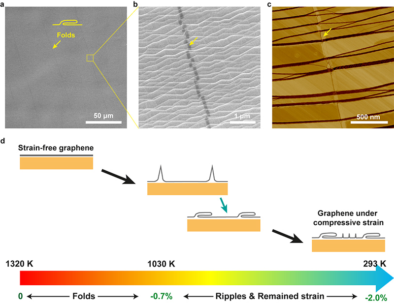
Figure 1. (a, b) SEM images and (c) AFM phase image of graphene folds in an adlayer-free single-crystal graphene film on a Cu(111) foil. (d) Schematic of the mechanism of graphene folds formation during the cooling process.
CMCM researchers first implemented a series of ‘cycling’ experiments that involved “cycling” the temperature immediately after growing the graphene at 1320 K. These experiments showed that the folds are formed at or above 1020 K during the cooling process. After learning this, the team decided to grow graphene on Cu-Ni(111) foils at several different temperatures around 1020 K, which led to a discovery that large-area, high-quality, fold-free, and adlayer-free single-crystal graphene films can be grown in a temperature range between 1000 K and 1030 K. “This fold-free graphene film forms as a single crystal over the entire growth substrate because it shows a single orientation over a large-area low-energy electron diffraction (LEED) patterns,” noted SEONG Won Kyung, a senior research fellow in CMCM who installed the LEED equipment in the center. GFETs were then patterned on this single-crystal fold-free graphene in a variety of directions by UNIST graduate student Yunqing Li. These GFETs showed remarkably uniform performance with average room temperature electron and hole mobilities of 7.0 ± 1.0 × 103 cm2 V-1 s-1. Li notes, “Such remarkably uniform performance is possible because the fold-free graphene film is a single crystal with essentially no imperfections.”
Importantly, the research team was able to achieve “scaling up” of graphene production using this method. The graphene was successfully grown on 5 foils (dimension 4 cm x 7 cm) simultaneously in a 6-inch diameter home-built quartz furnace. “Our method of growing fold-free graphene films is very reproducible, with each foil yielding two identical pieces of high-quality graphene films on both sides of the foil,” and “By using the electrochemical bubbling transfer method, graphene can be delaminated in about 1 minute and the Cu-Ni(111) foil can be quickly readied for the next growth/transfer cycle,” notes Meihui Wang. Ming Huang adds, “When we tested the weight loss of Cu-Ni(111) foils after 5 runs of growth and transfers, the net loss was only 0.0001 grams. This means that our growth and transfer methods using the Cu-Ni(111) can be performed repeatedly, essentially indefinitely.”
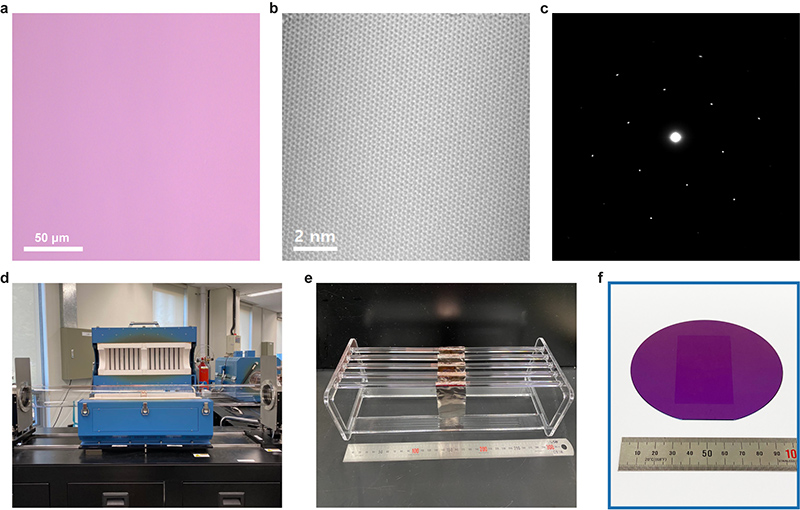
Figure 2. (a) Optical image, (b) atomic resolution TEM (transmission electron microscope) image, and (c) representative selected area electron diffraction (SAED) pattern of a fold-free adlayer-free graphene film grown on Cu-Ni(111) foil made by the CMCM. (d) A 6-inch quartz tube CVD furnace system used to evaluate scalable production of single-crystal fold-free graphene films on single-crystal Cu-Ni(111) alloy foils. (e) 5 pieces of 4 cm × 7 cm Cu-Ni(111) alloy foils were hung on a quartz holder and graphene was grown on both sides of each foil. (f) Photograph of the 4 cm × 7 cm fold-free single-crystal graphene film grown in the 6-inch CVD system shown in (e) and then transferred onto a 4-inch diameter silicon wafer.
In the process of achieving fold-free single-crystal graphene, the researchers also discovered the reasons behind the formation of these folds. High-resolution TEM imaging was performed by student CHOE Myeonggi and Prof. LEE Zonghoon (a group leader in CMCM and professor at UNIST) to observe the cross-sections of the samples grown above 1040 K. They discovered that the deadhesion, which is the cause of the folds, is initiated at the “bunched step edge” regions between the single crystal Cu-Ni(111) plateaus. “This deadhesion at the bunched step edge regions triggers the formation of graphene folds perpendicular to the step edge direction”, noted co-corresponding author Luo. Ruoff further notes that “We discovered that step-bunching of a Cu-Ni(111) foil surface suddenly occurs at about 1030 K, and this ‘surface reconstruction’ is the reason why the critical growth temperature of fold-free graphene is at ~1030 K or below”.
Such large-area fold-free single-crystal graphene film allows for the straightforward fabrication of integrated high-performance devices oriented in any direction over the entire graphene film. These single-crystal graphene films will be important for further advances in basic science, which will lead to new applications in electronic, photonic, mechanical, thermal, and other areas. The near-perfect graphene is also useful for stacking, either with itself and/or with other 2D materials, to further expand the range of likely applications. Given that the Cu-Ni(111) foils can be used repeatedly and that the graphene can be transferred to other substrates in less than one minute, the scalable manufacturing using this process is also highly promising.
A further interesting aspect of this article is that it includes Nature’s “Transparent Peer Review” document, so that readers may read through the reviewer comments and author rebuttals to also “observe” the process of scientific review. The paper went through two cycles of review and thus three revisions of the main text and the Supplemental Information document prior to being accepted. When the review process “works well”, reviewers offer useful comments and questions that the authors can then ponder and try to answer. Ruoff and Luo noted that “We dived back into our labs at the CMCM and really worked hard to respond to the reviewer comments and also to tackle other interesting aspects of the science during the 6-month time between our originally submitted manuscript to Nature, and its acceptance after 3 rounds of revision.” Ruoff further notes, “This was like a huge breath of fresh air for us— we got professional reviews and the entire review experience was professional in all regards. I think the “Transparent Peer Review” played a role in achieving this proper level of professionalism. Other journals might take note.”
Read the original article on IBS.