
The ability to develop inexpensive, efficient, designer infrared light sources could revolutionize molecular sensing technologies. Additional applications include free-space communications, infrared beacons for search and rescue, molecular sensors for monitoring industrial gases, environmental pollutants and toxins.
The research team’s approach, detailed today in Nature Materials, uses simple thin-film deposition, one of the most mature nano-fabrication techniques, aided by key advances in materials and machine learning.
Standard thermal emitters, such as incandescent lightbulbs, generate broadband thermal radiation that restricts their use to simple applications. In contrast, lasers and light emitting diodes offer the narrow frequency emission desired for many applications but are typically too inefficient and/or expensive. That has directed research toward wavelength-selective thermal emitters to provide the narrow bandwidth of a laser or LED, but with the simple design of a thermal emitter. However, to date most thermal emitters with user-defined output spectral have required patterned nanostructures fabricated with high-cost, low-throughput methods.
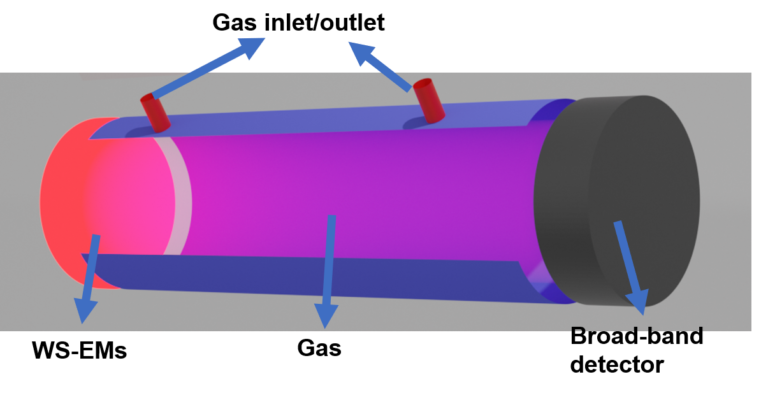
Schematic of a filterless, non-dispersive infrared sensor enabled by the research team’s advanced infrared light source. Illustration by Mingze He, Caldwell group
The research team led by Joshua Caldwell, Vanderbilt associate professor of mechanical engineering, and Jon-Paul Maria, professor of materials science and engineering at Penn State, set out to conquer long-standing challenges and create a more efficient process. Their approach leverages the broad spectral tunability of the semiconductor cadmium oxide in concert with a one-dimensional photonic crystal fabricated with alternating layers of dielectrics referred to as a distributed Bragg reflector.
The combination of these multiple layers of materials gives rise to a so-called “Tamm-polariton,” where the emission wavelength of the device is dictated by the interactions between these layers. Until now, such designs were limited to a single designed wavelength output. But creating multiple resonances at multiple frequencies with user-controlled wavelength, linewidth, and intensity is imperative for matching the absorption spectra of most molecules.
Material design has been challenging and computationally intense. Because advanced applications require functionality at multiple resonances, the new process had to drastically shorten design time. A typical device, for example, would contain tens to hundreds of designable parameters, creating high customization demands requiring unrealistic computation times. For instance, in a scenario that independently optimizes nine parameters, sampling 10 points per parameter, the simulations would take 15 days assuming 100 simulations each second. Yet, with more parameters, the time increases exponentially—11 and 12 parameters would require three and 31 years, respectively.
To address this challenge, PhD student Mingze He, lead author of the paper, proposed an inverse design algorithm that computes an optimized structure within minutes on a consumer-grade desktop. Further, this code could provide the ability to match the desired emission wavelength, linewidth, and amplitude of multiple resonances simultaneously over an arbitrary spectral bandwidth.
Another hurdle was identifying a semiconductor material that could allow a large dynamic range of electron densities. For this, the team used doped semiconductor material, developed by Maria’s research team at Penn State, that allows intentional design of optical properties.
“This allows the fabrication of advanced mid-infrared light sources at wafer-scale with very low cost and minimal fabrication steps,” He said.
This experimental section was conducted with Penn State collaborators while the devices were characterized by He and J. Ryan Nolen, a recent graduate of the Caldwell group. Together, the two teams successfully demonstrated the capability of inversely designed infrared light sources.
“The combination of the cadmium oxide material tunability with the fast optimization of aperiodic distributed Bragg reflectors offers the potential to design infrared light sources with user-defined output spectra. While these have immediate potential in chemical sensing, these also exhibit significant promise in a variety of other applications ranging for environmental and remoted sensing, spectroscopy, and infrared signaling and communications.” Caldwell said.
Significantly, the Caldwell group has open-sourced the design algorithm, which can be downloaded on the Nature Materials as well as the Caldwell Infrared Nanophotonic Materials and Devices laboratory website.
Their paper, “Deterministic inverse design of Tamm plasmon thermal emitters with multi-resonant control,” was published Oct. 21. Funding sources included the Office of Naval Research, Army Research Office, National Defense Science and Engineering Graduate Fellowship, and the National Science Foundation.
Read the original article on Vanderbilt University.