
Researchers from the Low Energy Electronic Systems (LEES) interdisciplinary research group at the Singapore-MIT Alliance for Research and Technology (SMART), MIT’s research enterprise in Singapore, together with collaborators at MIT, National University of Singapore (NUS), and Nanyang Technological University (NTU), have discovered a new method of generating long-wavelength (red, orange, and yellow) light using intrinsic defects in semiconducting materials, with potential applications as direct light emitters in commercial light sources and displays. This technology would be an improvement on current methods, which use phosphors, for instance, to convert one color of light to another.
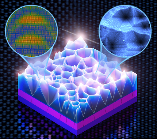
A new method of quantum dot fabrication makes use of intrinsic defects in LED materials. By forming pyramids, localized bright luminescence emanates from the apexes containing indium-rich quantum dots.
A type of group-III element nitride-based light-emitting diode (LED), indium gallium nitride (InGaN) LEDs were first fabricated over two decades ago in the 1990s, and have since evolved to become ever-smaller while growing increasingly powerful, efficient, and durable. Today, InGaN LEDs can be found across myriad industrial and consumer use cases, including signals and optical communication and data storage — and are critical in high-demand consumer applications such as solid state lighting, television sets, laptops, mobile devices, and augmented- and virtual-reality solutions.
Ever-growing demand for such electronic devices has driven over two decades of research into achieving higher optical output, reliability, longevity, and versatility from semiconductors — leading to the need for LEDs that can emit different colors of light. Traditionally, InGaN material has been used in modern LEDs to generate purple and blue light, with aluminium gallium indium phosphide (AlGaInP) — a different type of semiconductor — used to generate red, orange, and yellow light. This is due to InGaN’s poor performance in the red and amber spectrum caused by a reduction in efficiency as a result of higher levels of indium required.
In addition, such InGaN LEDs with considerably high indium concentrations remain difficult to manufacture using conventional semiconductor structures. As such, the realization of fully solid-state white-light-emitting devices — which require all three primary colors of light — remains an unattained goal.
Addressing these challenges, SMART researchers have laid out their findings in a paper titled “Light-Emitting V-Pits: An Alternative Approach toward Luminescent Indium-Rich InGaN Quantum Dots,” recently published in the journal ACS Photonics. In their paper, the researchers describe a practical method to fabricate InGaN quantum dots with significantly higher indium concentration by using preexisting defects in InGaN materials.
In this process, the coalescence of so-called V-pits, which result from naturally existing dislocations in the material, directly forms indium-rich quantum dots, small islands of material that emit longer-wavelength Growing these structures on conventional silicon substrates further eliminates the need for patterning or unconventional substrates. The researchers also conducted high spatially resolved compositional mapping of the InGaN quantum dots, providing the first visual confirmation of their morphology.
In addition to the formation of quantum dots, the nucleation of stacking faults — another intrinsic crystal defect — further contributes to emissions of longer wavelengths.
Jing-Yang Chung, SMART graduate student and lead author of the paper, says, “For years, researchers in the field have attempted to tackle the various challenges presented by inherent defects in InGaN quantum-well structures. In a novel approach, we instead engineered a nano-pit defect to achieve a platform for direct InGaN quantum dot growth. As a result, our work demonstrates the viability of using silicon substrates for new indium-rich structures which, along with addressing current challenges in the low efficiencies of long-wavelength InGaN light emitters, also alleviate the issue of expensive substrates.”
In this way, SMART’s discovery represents a significant step forward in overcoming InGaN’s reduced efficiency when producing red, orange and yellow light. In turn, this work could be instrumental in developing future micro LED arrays consisting of a single material.
Silvija Gradečak, co-author and principal investigator at LEES, adds, “Our discovery also has implications for the environment. For instance, this breakthrough could lead to a more rapid phasing out of non-solid-state lighting sources — such as incandescent bulbs — and even the current phosphor-coated blue InGaN LEDs with a fully solid-state color-mixing solution, in turn leading to a significant reduction in global energy consumption.”
“Our work could also have broader implications for the semiconductor and electronics industry, as the new method described here follows standard industry manufacturing procedures and can be widely adopted and implemented at scale,” says SMART CEO and LEES Lead Principal Investigator Eugene Fitzgerald. “On a more macro level, apart from the potential ecological benefits that could result from InGaN-driven energy savings, our discovery will also contribute to the field’s continued research into and development of new efficient InGaN structures.”
The research is carried out by SMART and supported by the National Research Foundation (NRF) Singapore under its Campus for Research Excellence and Technological Enterprise (CREATE) program. For this paper, the LED structures were grown using SMART’s unique facilities and know-how, structural studies were conducted at NUS using state-of-the-art, atomically-resolved electron microscopes, while nanoscale optical studies were conducted at MIT and NTU.
LEES is creating new integrated circuit technologies that result in increased functionality, lower power consumption and higher performance for electronic systems. These integrated circuits of the future will impact applications in wireless communications, power electronics, LED lighting, and displays. LEES has a vertically-integrated research team possessing expertise in materials, devices, and circuits, comprising multiple individuals with professional experience within the semiconductor industry. This ensures that the research is targeted to meet the needs of the semiconductor industry both within Singapore and globally.
SMART was established by MIT and the NRF in 2007. SMART is the first entity in CREATE developed by NRF and serves as an intellectual and innovation hub for research interactions between MIT and Singapore, undertaking cutting-edge research projects in areas of interest to both. SMART currently comprises an Innovation Center and five interdisciplinary research groups: Antimicrobial Resistance, Critical Analytics for Manufacturing Personalized-Medicine, Disruptive & Sustainable Technologies for Agricultural Precision, Future Urban Mobility, and LEES.
Read the original article on Massachusetts Institute of Technology (MIT).