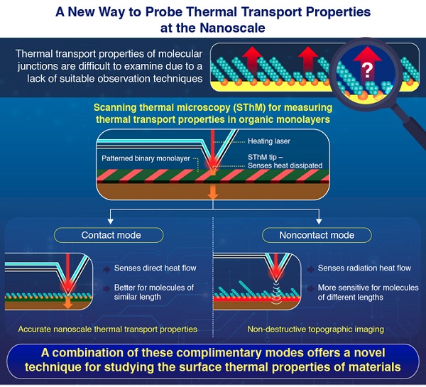
In a few studies, scientists managed to measure the thermal transport properties in molecular junctions at the nanoscale using a technique called scanning thermal microscopy (SThM). This method involves putting a very sharp metallic tip in contact with the target material and moving this tip throughout the material’s surface. The tip, which is heated from behind using a laser, contains a thermocouple. This small device measures temperature differences and so, by balancing the heating of the tip caused by the laser with the tip’s cooling caused by heat flowing into the target sample, it becomes possible to measure a material’s thermal transport characteristics point by point.

In a recent study published in Journal of the American Chemical Society, scientists from Tokyo Tech reported a serendipitous yet important finding while using SThM. The team was employing a SThM technique to measure the thermal transport properties of self-assembled monolayers (SAMs). These samples contained alternating stripes of each of the three possible pairs between n-Hexadecanethiol, n-Butanethiol, and Benzenethiol. Besides employing the standard contact-based SThM approach, the researchers tried using a non-contact regime as well, in which the tip of the scanning thermal microscope was kept above the sample without touching it. Unexpectedly, they realized this non-contact regime had some serious potential.
In the contact SThM regime, heat flows directly from the tip to the sample. By contrast, in the non-contact SThM regime, the only heat transfer between the tip and the sample occurs via heat radiation. As the team found out through experiments, while the contact regime is best for visualizing the thermal transport characteristics, the non-contact regime is much more sensitive to the actual length of the molecules ‘sticking out’ from the substrate. Thus, the combination of the non-contact and contact regimes provides an all-new way of creating topographic and thermal transport images of a sample simultaneously.
Moreover, the non-contact approach has advantages over other well-established microscopy techniques, as Associate Professor Shintaro Fujii, lead author of the paper, explains: “The non-contact SThM approach is completely non-destructive, unlike other techniques like atomic force microscopy, which does require contact between the scanning tip and the sample and thus has a mechanical impact that can damage soft organic materials.”
Overall, the insight provided by this study will pave the way to novel technological advances and a deeper comprehension of materials at the nanoscale. “Our work not only is the first to provide thermal images of organic SAMs, but also provides a new technique for investigating thermal transport properties, which will be essential for thermal management in various types of nanodevices,” concludes Fujii.
Read the original article on Tokyo Institute of Technology.
