
Nanomaterials are materials that, by definition, have an external dimension of as low as 1 – 1000 nanometers in at least one dimension. However, these "midgets" have a strong impact in a wide range of applications, from cosmetics to aerospace to consumer goods, and in the energy and electronics sectors. For example, perovskite coatings are highly suitable for the production of thin film solar cells with high efficiencies and low manufacturing costs. Vacuum coating processes are used, for example, to functionalize plastic films on the surface with a permeation barrier layer against water or oxygen. Thermally reflective coatings (low-E) on film or glass are used, for example, in the automotive industry and for saving energy in buildings.
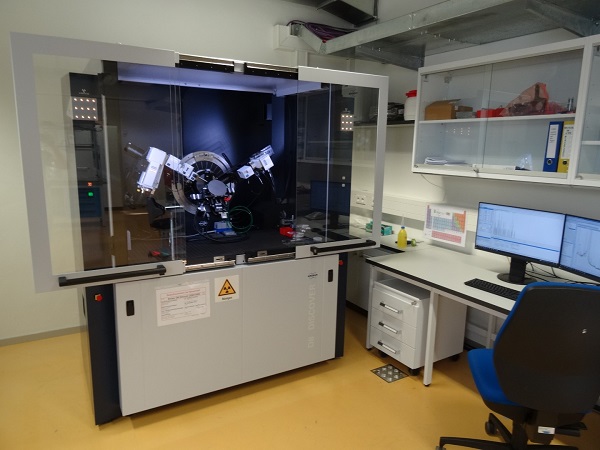
XRR and XRD for at-line quality control at Fraunhofer FEP.
The functional properties of these thin films with nanometer-scale thickness are determined not only by the selection of materials, but also by their nano-physical dimensions, structure and chemical composition. Precise characterization of these properties is crucial for the development of new functional nanomaterials and the optimization of processes for higher performance, more efficient manufacturing processes and material yields, and scaling up to larger volumes.
X-ray characterization techniques such as X-ray diffraction (XRD) or X-ray reflectometry (XRR) are widely used in research laboratories for these tasks, but are rarely used in industrial materials development and production process evaluation due to technical limitations and the high level of expertise required. Hyperspectral imaging has also proven to be a useful tool for thin film characterization in laboratory environments. Unlike a RGB photo camera, which records an image in only three colors (red, green, blue), a hyperspectral camera is able to record an image in hundreds of different “colors” in the visible and short-wave infrared spectral region at the same time, such that each pixel within the image contains the complete spectral information of a scene. This additional information enables the detection and visualization of even small differences in the layer properties.
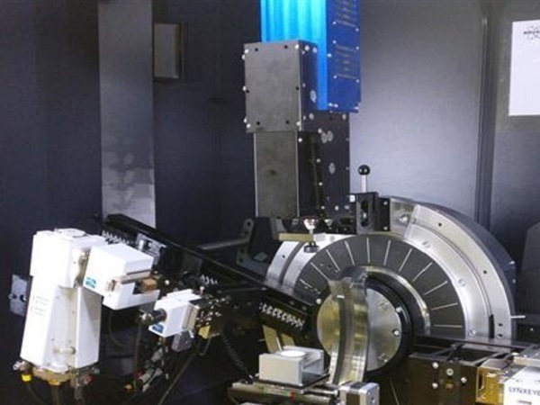
In-situ superposition of CRD and HSI property imaging at Bruker AXS.
The European nanomaterials market is forecast to generate revenues of around USD 9.1 billion by 2022 and grow at a rate of 20.0 % between 2016 and 2022 (source: Matec Conferences). Enterprises using and producing nanomaterials are therefore faced with a constantly increasing demand for fast and reliable process and product quality control. This requires industry-ready real-time measurements and process-adapted monitoring capabilities.
This is where the NanoQI project, funded by the European Union with Horizon 2020 funds, comes in. The consortium of eight companies and organizations from five European countries already started on March 1, 2020, to develop an industry-ready, real-time and in-line capable method for characterizing and imaging nano-dimensions of (thin film) nanomaterials in the critical range of 1 to 300 nm on large sample surfaces of more than 500 × 500 mm². For this purpose, NanoQI combines for the first time X-ray reflectometry (XRR) and X-ray diffraction analysis (XRD) as well as broadband hyperspectral imaging (HSI) into a fast, real-time method for quality control in thin film processing that can be directly integrated into the coating equipment. This combination enables equipment operators to access application-relevant properties such as the thickness of individual layers in a coating system, the solid state structure or even derived functional properties – such as water vapor permeability – while the coating is still in progress.
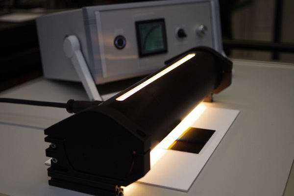
HSI hardware integration and algorithms for automatic quality assessment using HSI, based on XRR/XRD- ground-truth data.
Project coordinator Dr. John Fahlteich explains how the NanoQI solution will be validated: "In order to develop a truly industry-ready and real-time as well as in-line capable characterization solution for nanomaterials, we are testing it in three industry relevant use cases with a high demand for real-time characterization." These application areas are nano-crystalline perovskite films for high-efficiency solar cells, transparent conductive layer systems on plastic films for flexible electronics, and large-area atomic layer deposition of dielectric or encapsulation layers. All three systems benefit from in-line quality monitoring and imaging evaluation of the homogeneity and long-term stability of the layer properties. They also represent fast-growing subsectors of thin film and nanotechnology, with many European companies active in this field. Therefore, NanoQI contributes significantly to Europe's industrial competitiveness.
An External Advisory Board composed of well-known experts secures close interaction with industry, in particular machine manufacturers, material suppliers, production companies and future users who can benefit from NanoQI technology. Also, the NanoQI consortium closely interacts with representatives of standardization bodies (IEC TC113 and TC119, ISO TC229), certification bodies for regulation and radiation protection (e. g. TÜV), thin film industry associations and scientific experts for material analysis.
Upon project mid-term in September 2021, the project partners were able to commission the first instrument prototypes, that were assembled by Bruker AXS (Germany) and Norsk Elektro Optikk AS (Norway) specifically for the requirements of the project. A combined X-ray diffractometer (XRD) and X-ray reflectometer (XRR) has been installed at Fraunhofer FEP in Dresden (Germany). Another XRD unit was integrated into a machine for the production of thin film perovskite solar cells for the first time at the project partner TNO (Netherlands). With these devices, layer thickness and nanometer scale roughness, as well as crystallinity of thin layers or layer stacks can be measured very precisely and at high speed.
The material data obtained in this way will serve as the basis for the generation of optical models for high-resolution HSI analysis of large coated substrate areas. NanoQI relies on the expertise of Fraunhofer IWS (Germany) and Nork Elektro Optikk for the integration of the HSI components as well as the analysis of the large amount of data generated from an HSI measurement. Machine learning algorithms are being implemented to further accelerate the data analysis and to enable the determination of derived functional properties of the layers from the HSI image data. The HSI camera prototypes will be installed and commissioned at the partners' facilities starting in November 2021. Subsequently, the methods will be tested and further optimized in the operational use of the coating systems.
In future, the combination of XRD, XRR and HSI integrated into thin film processing machines will significantly simplify quality control and process monitoring in the industrial production. For example, coating machines could use the NanoQI technology to gather and process large amounts of spatially resolved data about surface properties of the coated substrate in real-time during the deposition process – displaying even small deviations in an easy-to-evaluate false color image. This would, for example, enable rapid optimization of the process parameters to achieve the desired layer properties and targeted homogeneity. Likewise, yield in manufacturing is increased because process parameters can be readjusted at an early stage - before the layer properties run out of specification.
Read the original article on Fraunhofer FEP.