
This property is known as negative refraction and it means that the refractive index—the speed that light can travel through a given material—is negative across a portion of the electromagnetic spectrum at all angles.
Refraction is a common property in materials; think of the way a straw in a glass of water appears shifted to the side, or the way lenses in eyeglasses focus light. But negative refraction does not just involve shifting light a few degrees to one side. Rather, the light is sent in an angle completely opposite from the one at which it entered the material. This has not been observed in nature but, beginning in the 1960s, was theorized to occur in so-called artificially periodic materials—that is, materials constructed to have a specific structural pattern. Only now have fabrication processes have caught up to theory to make negative refraction a reality.
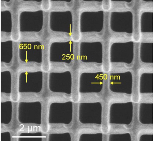
Scanning Electron Microscopy (SEM) image of the nanoscale lattice.
"Negative refraction is crucial to the future of nanophotonics, which seeks to understand and manipulate the behavior of light when it interacts with materials or solid structures at the smallest possible scales," says Julia R. Greer, Caltech's Ruben F. and Donna Mettler Professor of Materials Science, Mechanics and Medical Engineering, and one of the senior authors of a paper describing the new material. The paper was published in Nano Letters on October 21.
The new material achieves its unusual property through a combination of organization at the nano- and microscale and the addition of a coating of a thin metal germanium film through a time- and labor-intensive process. Greer is a pioneer in the creation of such nano-architected materials, or materials whose structure is designed and organized at a nanometer scale and that consequently exhibit unusual, often surprising properties—for example, exceptionally lightweight ceramics that spring back to their original shape, like a sponge, after being compressed.
Under an electron microscope, the new material's structure resembles a lattice of hollow cubes. Each cube is so tiny that the width of the beams making up the cube's structure is 100 times smaller than the width of a human hair. The lattice was constructed using a polymer material, which is relatively easy to work with in 3-D printing, and then coated with the metal germanium.
"The combination of the structure and the coating give the lattice this unusual property," says Ryan Ng (MS '16, PhD '20), corresponding author of the Nano Letters paper. Ng conducted this research while a graduate student in Greer's lab and is now a postdoctoral researcher at the Catalan Institute of Nanoscience and Nanotechnology in Spain. The research team zeroed in on the cube-lattice structure and material as the right combination through a painstaking computer modeling process (and the knowledge that geranium is a high-index material).
To get the polymer coated evenly at that scale with a metal required the research team to develop a wholly new method. In the end, Ng, Greer, and their colleagues used a sputtering technique in which a disk of germanium was bombarded with high-energy ions that blasted germanium atoms off of the disk and onto the surface of the polymer lattice. "It isn't easy to get an even coating," Ng says. "It took a long time and a lot of effort to optimize this process."
The technology has potential applications for telecommunications, medical imaging, radar camouflaging, and computing.
In 1965 observation, Caltech alumnus Gordon Moore (PhD '54), a life member of the Caltech Board of Trustees, predicted that integrated circuits would get twice as complicated and half as expensive every two years. However, because of the fundamental limits on power dissipation and transistor density allowed by current silicon semiconductors, the scaling predicted by Moore's Law should soon end. "We're reaching the end of our ability to follow Moore's Law; making electronic transistors as small as they can go," Ng says. The current work is a step towards demonstrating optical properties that would be required to enable 3-D photonic circuits. Because light moves much more quickly than electrons, 3-D photonic circuits, in theory, would be much faster than traditional ones.
Read the original article on California Institute of Technology (Caltech).