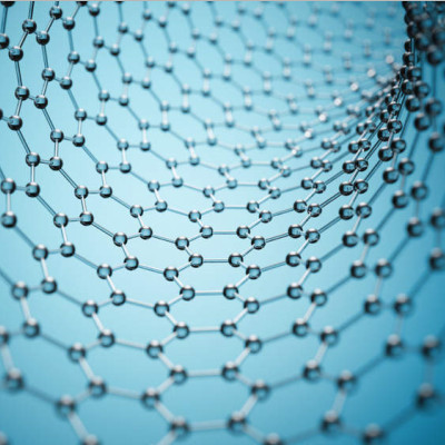
Graphene is the one-atom-thick layer of carbon atoms, known as the world's thinnest material. The material has become a popular choice in semiconductor, automotive and optoelectronic industry due to its excellent electrical, chemical, and material properties. One such property is its extremely high carrier mobility.
“In solid-state physics, the electron carrier mobility characterizes how quickly an electron can move through a metal or semiconductor when pulled by an electric field. The high electron mobility of graphene points to great potential for broadband communications and high-speed electronics operating at terahertz switching rates. In addition, the other material properties, such as high chemical stability, excellent transparency, and electrical sensitivity towards biochemicals, make it a promising material for displays, light harvesting devices and biosensors”, says Munis Khan.
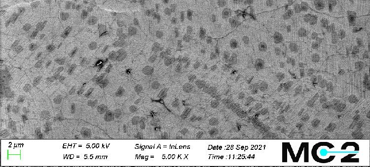
However, the extremely high carrier mobility in graphene is either observed in mechanically exfoliated graphene, a process that lacks industrial scalability, or graphene devices fabricated on hexagonal-boron nitride. Such high mobilities have also been observed by transferring graphene grown by a process called chemical vapor deposition (CVD) to complex-oxide heterostructures. All these techniques require complex and expensive fabrication methods, which not only makes it more expensive but also hinder mass production of such devices.
Cheaper graphene with high carrier mobility
Now, Munis Khan and his colleagues report on a surprisingly high charge-carrier mobility of CVD graphene grown on unpolished copper foil and transferred to EVA/PET lamination foil by using an ordinary office laminator and wet etching of copper. The mobility increased up to eight times after simply holding the graphene-on-plastic sandwich at 60 C for a few hours.
“This finding shows that even cheap and flexible graphene devices can still have an uncompromisingly high mobility”, says Munis Khan. “Our article proposes a straightforward method to fabricate cheap graphene devices on flexible substrates with high carrier mobility, probably only limited by the CVD process and purity of copper.”
CVD graphene transferred to EVA/PET is being intensely explored and studied for flexible and stretchable electronics, especially in shape-conforming systems such as portable energy-harvesting devices, electronic skin, and wearable electronic devices, which need high flexibility and stretchability. Conventional semiconductors lack the superior mechanical properties that graphene possesses, which makes them unsuitable for such applications – often highly conductive flexible graphene films possessing high carrier mobility are required.
“Our observation will indeed increase the scope of such flexible graphene films in this field. This could also usher the new era of flexible electronics. Applications requiring highly conductive thin films can now be realized by an affordable and simple method as proposed in our article. Indeed, in our research group we intend to use such graphene films for making extremely sensitive biosensors, terahertz detectors and high frequency devices, applications that too requires high carrier mobility. The challenge will be to integrate microfabrication techniques to make devices on flexible substrates. Once such issues are addressed, probably within 2-3 years, we can start utilizing such graphene films to fabricate devices for industrial use”, says Munis Khan.
Read the original article on Chalmers University of Technology.