
This hybrid material possesses valuable properties towards use in future memory and electronic devices such as TVs, computers and phones. Most significantly, the electronic properties of the new stacked structure can be controlled without the need for external strain, opening the way for use in future low-energy transistors.
The result is a new potential material for multiferroic nanodevices, such as field-effect transistors and memory devices, which could operate using much less energy than current silicon-based electronics as well as making electronic components smaller.
Atomically-thin building blocks
The work uses a structure comprising two atomically-thin materials: a film of a ferroelectric material, and another film of a magnetic material. (Such a structure of two or more different materials is referred to as a ‘heterostructure’.)
By stacking the two 2D materials together, the researchers create a ‘multiferroic’ material that combines the unique properties of the component ferroelectric and ferromagnetic materials.
– Ferromagnetic (or magnetic) materials are familiar, as materials with a permanent, intrinsic magnetism, such as iron. In ferromagnetic materials, electron spin can be aligned to form a strong magnetic field (this is what it means that they can be ‘magnetised’).
– Ferroelectric materials can be considered the electrical analogy to ferromagnetic materials, with their permanent electric polarisation resembling the north and south poles of a magnet.
– Multiferroic materials are simply those that exhibit more than one ferroic property (in this case, ferromagnetism and ferroelectricity).
Specifically, the researchers found they could use the intrinsic ferroelectric properties to tune the Schottky barrier height of the In2Se3/ Fe3GeTe2 heterostructure rather than using applied strain, that is required by other systems. (The Schottky barrier is an energy difference created by joining a metal with a semiconductor.)
Being able to tune the height of the barrier is needed to convert current from alternating (AC) to direct (DC) for use in electronic components such as diodes which are found in TVs, computers and other everyday electronic devices.
The resulting, switchable Schottky barrier structure can form an essential component in a two-dimensional field-effect transistor (FET) that can be operated by switching the intrinsic ferroelectric polarisation, rather than by the application of external strain.
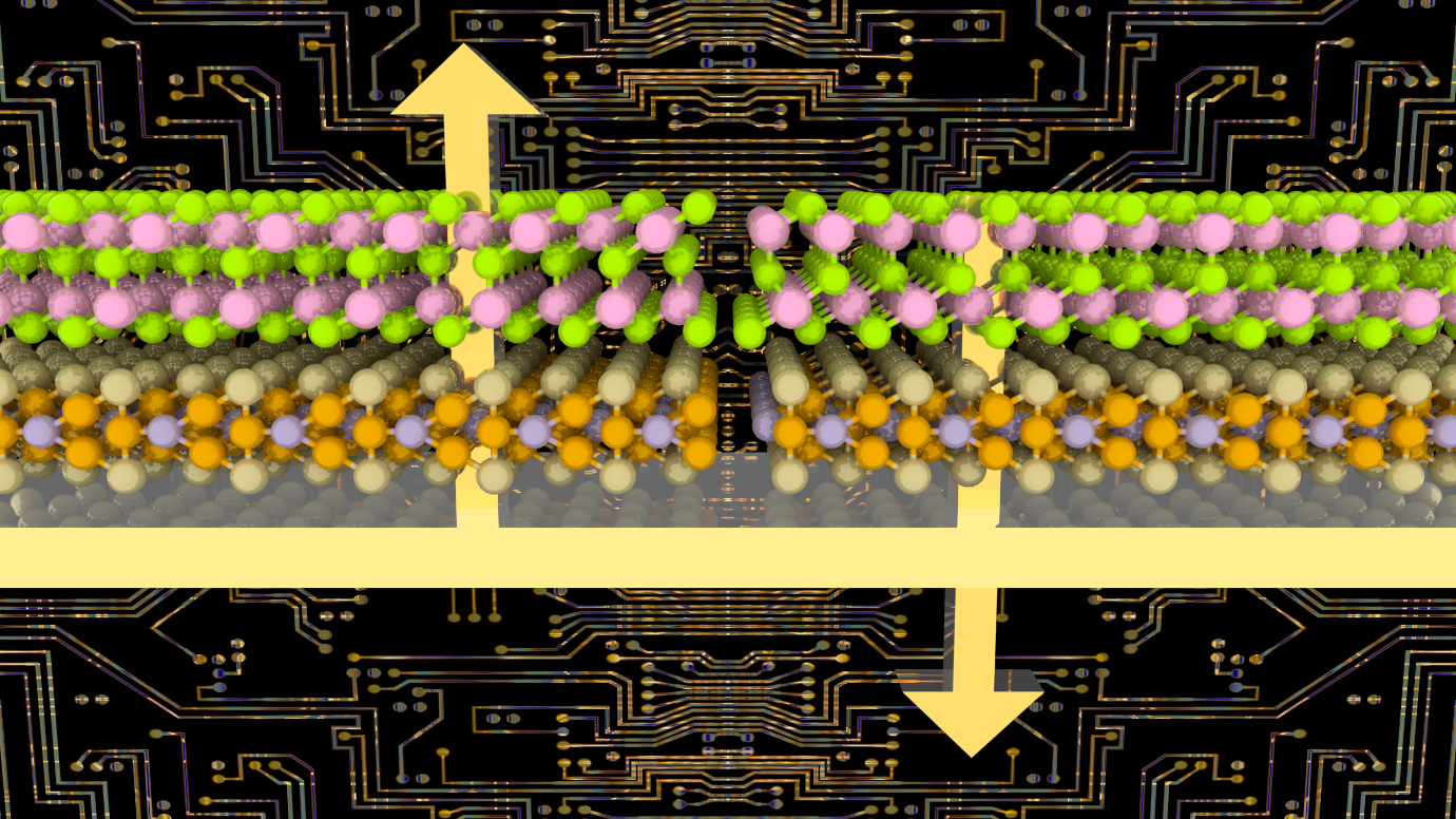
The switchable 2D Schottky diode device is formed by the interface of the 2D metal FGT (lower layer) and the 2D ferroelectric In2Se3 (upper layer).
Switching without external strain
This work employs a heterostructure of two 2D monolayers: In2Se3 and Fe3GeTe2 (usually abbreviated to ‘FGT’), where In2Se3 is a ferroelectric semiconductor and FGT is a magnetic/ferromagnetic material.
“Our findings show that the In2Se3/FGT provides properties comparable to other heterostructures but without the need of external strain,” says corresponding author Prof Michelle Spencer. “Not only can we control the barrier height with this heterostructure, but we can also switch between an n-type and p-type Schottky barrier.”
Such controllability and tunability of the In2Se3/FGT heterostructure can substantially broaden its device potential in future low-energy electronic devices.
“We found a significant change in the structural and electronic properties switching between the configurations of In2Se3. Such changes make this heterostructure useful as a switchable 2D Schottky diode device,” said lead author Dr Maria Javaid.
From theory to the lab
The finding is directly applicable to FLEET’s mission towards a new generation of ultra-low energy technologies beyond CMOS electronics.
As well as introducing a new possible avenue towards multiferroic nanodevices, the work will motivate experimentalists in this field to explore further opportunities for the use of In2Se3/FGT in future low-energy electronic devices, for example:
Synthesising a new multiferroic heterojunction that has the ability to ‘tune’ the Schottky barrier height, and switch between an n-type and p-type, via a switch in ferroelectric polarisation.
Exploring heterostructures of In2Se3 with other ferromagnetic materials.
The study
Tuning the Schottky barrier height in a multiferroic In2Se3/Fe3GeTe2 van der Waals heterojunction has just been published in Nanoscale Volume 14 Issue 11 in March 2022.
Read the original article on ARC Centre of Excellence in Future Low-Energy Electronics Technologies (FLEET).