
“We used a transmission electron microscope, which has been used extensively for imaging materials at the molecular, granular or sub-granular level, to help us understand how these materials behave, because in the electron microscope the electron beam wavelength can probe smaller distances than the visible light microscope,” said John Lambros, professor in the Department of Aerospace Engineering and director of the Advanced Materials Testing and Evaluation Laboratory at Illinois.
“Beyond imaging, however, we wanted to turn the electron microscope into a full-field metrology measurement instrument. Measurements in the electron microscope have been made before, but only at individual points through particle tracking. We added digital image correlation capabilities which we extended for use in this very high-magnification, high-resolution microscope instrument.”
Lambros explained that electron microscopes bring unique challenges for the digital, image correlation metrology that had to be overcome.
“Because instead of a light beam, you have an electron beam illuminating the sample, the transmission electron microscope is a much harsher environment. It’s very difficult to operate and it’s all done in vacuum,” he said. “Imaging is much more difficult and the samples are very small scale.”
The researchers first ion-milled a bend-beam from a bulk piece of silicon dioxide, a type of glass, in the Materials Research Laboratory’s focused ion beam facility. In a vacuum deposition chamber, a thin film of gold is deposited on the beam. Then, the sample is heated and the continuous film breaks up into little islands, which provide sufficient contrast to be visible on the silica sample in the electron microscope.
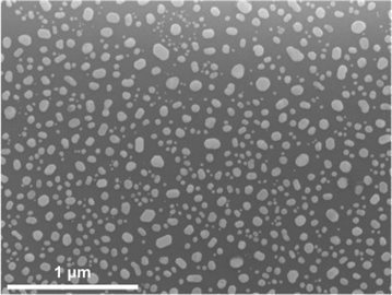
SEM image of gold particles formed on an SiO2 substrate via thermally induced de-wetting of a gold film.
“With a scanning electron microscope, the images are of the sample surface because the electron beam bounces off the surface,” Lambros said. “But in the transmission electron microscope the electron beam goes through the sample, which must be very thin, and the response is averaged through the thickness. Digital Image Correlation in the SEM has been used for a long time because it’s so much easier to get images there. This has not been done using the TEM, which has much higher magnification capabilities, and this is why we wanted to extend the digital image correlation method to the TEM.”
The researchers took images over time, up to 300 seconds, while the sample was subjected to a bending load, and compared image to image to measure how the gold particles deposited on the surface move.
“Digital image correlation takes a series of images of the gold dots as the loading is progressing. And by comparing one image to the next you can map what is happening—and not just around the edges, but internal features inside the sample,” Lambros said. “So, in this project, we used particle tracking as a check, or control, and then demonstrated the highly comparable results using digital image correlation in the TEM.”
Lambros explained that with particle tracking, there are typically fewer particles tracked which means fewer measurement points. And compared to DIC, the particle must move larger amounts for us to be able to see movement in an image.
“This study is about developing the digital image correlation method in the transmission electron microscope. Now that we have confirmation that the method works, we can replicate it and use it to study the nanoscale behavior of the spinel material, which was our initial interest,” Lambros said.
He said they have started the spinel studies by putting the gold particles to create a pattern on sample of spinel but have not tried it in the transmission electron microscope yet.
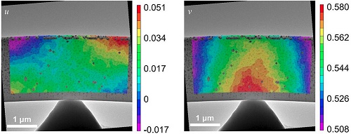
DIC contours of vertical (left) and horizontal (right) displacement during indentation of a SiO2 beam (values are in μm).
“The patterning works on spinel, but there will be other issues with spinel because it's crystalline and crystals behave very differently in the TEM than amorphous glass,” Lambros said. “In experimental mechanics one of our biggest constraints is that we mainly look at what's happening on the surface. We try to deduce from that what's happening inside the material and that's a difficult task. This method is really ground-breaking because now we’ll be able to image materials in a new way and at a very high magnification.”
Read the original article on University of Illinois.