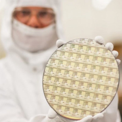
As one of five multi-project wafer (MPW) runs, this first phase is targeting sensor applications. Companies, universities and research institutes can include their designs as dies on joint wafers, to test their ideas for devices on a larger scale at relatively low costs.
The 2D-EPL is a €20 million project aiming to pioneer the fabrication of prototype electronics and sensors based on graphene and related materials (GRMs), and at integrating them into established silicon semiconductor platforms. The project will also help to refine and scale up the manufacturing process of graphene-based electronics, including developing critical tools, materials and processes.
The 2D-EPL includes partners from across the whole value chain – from tool manufacturers to semiconductor fabrication lines – including Chalmers University of Technology, Sweden; Aixtron, Germany and United Kingdom; Interuniversity Microelectronics Centre (imec), Belgium; AMO, Germany; VTT, Finland; Süss MicroTec, Germany; Graphenea, Spain; Micro Resist Technology, Germany; Innovations for High Performance Microelectronics (IHP), Germany, and Oxford Instruments, United Kingdom.
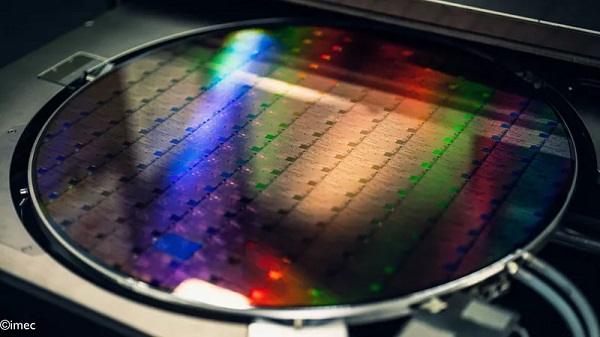
The 2D-EPL project will offer several kinds of integration services, including multi-project wafer (MPW ) runs. The first run will be hosted in AMO GmbH’s 400-m2 state-of-the art cleanroom. Target applications are bio, gas, or chemical sensor, hall sensor or photodetector applications, taking advantage of graphene’s extreme sensitivity to the environment. The baseline process is a graphene field effect transistor (GFET), with several customisation options.
The MPW run offers participants a chance to acquire GFETs on dies manufactured to their own designs. The cost of production is shared between the 2D-EPL project and the customer, meaning that users can access this technology at a much lower price point. At this time, the quantities available are suited for prototyping, research and development.
“This wafer run is a chance for academic groups, start-ups and other companies to test novel ideas for 2D material devices on a larger scale at relatively low costs,” explained Gordon Rinke, business developer at AMO. “As a result, they can collect more data of their devices and directly test a larger production volume — a necessary step to bringing a product to the market.”
“The MPW runs are an important step in the 2D-EPL project,” added 2D-EPL Division Leader, Cedric Huyghebaert. “Not only do they provide customers in both industry and academia with access to graphene-integrated wafers, but they offer an enormous learning opportunity with regards to the manufacturing of these devices. We plan to test and analyse every stage of the production process to scale up and improve the manufacturing of graphene-integrated electronics.”
The dies on the multi-project wafer are customisable within a set of specifications — size and certain critical dimensions are fixed, for example — and must be designed in accordance with the process design kit (PDK). AMO GmbH will support and collaborate with successful applicants on the design of the dies and offers a library of device designs to be used as a basis for modification.
“Electronics based on 2D materials can be a real vehicle for Europe to gain shares in the high-tech sector, but what is needed is the development of a whole ecosystem around this topic – from tool developers to potential customers. This is what the 2D-EPL is trying to achieve. At AMO, we are really excited to contribute our experience and our fabrication capabilities to this major project”, said Max Lemme, scientific director of AMO.
Read the original article on New Electronics.