
The rapid pace of technological change is clearly visible, but much of what you may not see, the exceedingly small physical components of change called nanotechnologies, are catalyzing the revolution. While there are many nanotech uses, three areas of nanotech are paving the way to our future: Materials Science, Nanomedicine and Device Engineering.
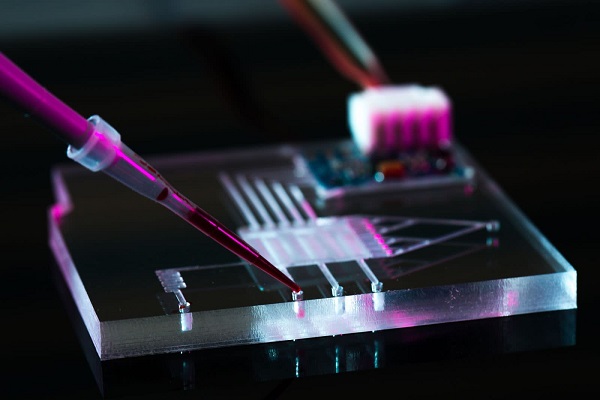
A lab-on-a-chip (LOC) is integration device with several laboratory functions
What is Nanotechnology?
The concept of nanotechnology was derived in 1959 by Nobel prize physicist Richard Feynman in a speech at the California Institute of Technology (Caltech). As further and more contemporarily defined by the National Nanotechnology Initiative (NNI), “Nanotechnology is the understanding and control of matter at the nanoscale, at dimensions between approximately 1 and 100 nanometers, where unique phenomena enable novel applications. Matter can exhibit unusual physical, chemical, and biological properties at the nanoscale, differing in important ways from the properties of bulk materials, single atoms, and molecules. Some nanostructured materials are stronger or have different magnetic properties compared to other forms or sizes of the same material. Others are better at conducting heat or electricity. They may become more chemically reactive, reflect light better, or change color as their size or structure is altered.”
Dr. Tom Cellucci, who, before he was appointed the First Chief Commercialization Officer of the United States by President George W. Bush (and re-appointed by President Obama), was an instrumental person in the creation of the NNI before he entered government service. He was determined, working with all three branches of the US Government, to get the $3.9 B in funding for the NNI, in order to start a nanotech revolution in our country and throughout the globe.
Dr. Cellucci offers insights into how nanotech is being integrated into the product development process. “Nanotechnology is being safely used today to protect people and structures through a systematic process of understanding detailed operational requirements and utilizing a detailed Technology Development process useable by both government and the private sector. This step-by-step process enables a thorough understanding of customers' requirements and execution of the commercialization of emerging technologies to provide stable and useful products.”
Dr. Cellucci has authored or co-authored more than 25 books and over 362 articles on requirements development, commercialization, nanotechnology, laser physics, and photonics. He’s recently turned his sights to working with one of his former undergraduate students at the University of Pennsylvania, Dr. Mark Banash (PhD Princeton University), at a small firm in the Boston area called JP Industries International, where they are developing and patenting a number of solutions for personal security and infrastructure protection applications using patented nanotech products and systems.
To get a better understanding of nanotech, it’s important to focus on the applications of nano particles. Nano particles are functional across a variety of industries and verticals. The graphic below is an excellent summary of those extensive applications:
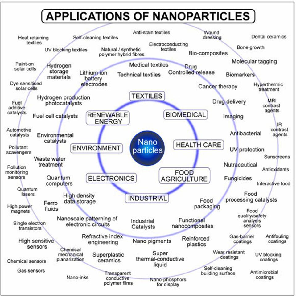
Applications of Nanoparticles. Source: "Commercial scale production of inorganic nanoparticles"
As nano particles are the building blocks of new discoveries, the graph above highlights many industries and verticals where nanotech may have applications. NNI notes that by using nanotechnology-based principals, materials can be made to be stronger, lighter, more durable, more reactive, and serve as better electrical conductors.
While the list of nanoparticle applications in the graphic are all important, three areas of are areas of nanotech are already impacting our future: 1– Materials Science (Construction), 2– Nanomedicine (and Health), and 3– Device Engineering (Electronics, Wearables).
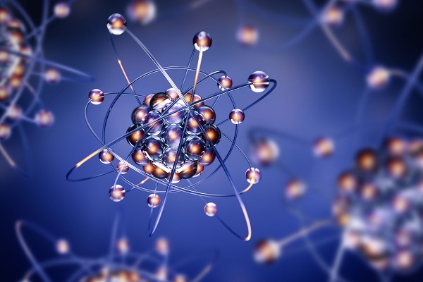
Atom, Molecule, Molecular Structure, Electron, Proton
Materials Science:
In industry, government and academia, new and exciting research in nano particles and materials science are creating stronger, durable, lighter, and even “self-healing” and self-assembling materials through nano-scale engineering. Nanomaterials artificially engineered as molecular scale synthetic composites are now being designed at the inter-atomic level.
The capability to use nano-mechanics to design and manufacture infrastructures such as bridges, roads, buildings — all with stronger, adaptable, self-intelligent, and seemingly mundane materials will revolutionize the construction and transportation industries. The Department of Energy and Department of Transportation have many programs and initiatives in material sciences in progress.
Via the use of nanoparticles, 3D Printing and 4D Self-assembling Printing are accelerating material science. 3-D Printing is trailblazing future manufacturing by using creations of material science. 3-D Printing connotes a three-dimensional object that is created layer by layer via computer aided design programs. To be able to print the object, the computer divides it into flat layers that are printed one by one. By printing with advanced pliable materials such as plastics, ceramics, metals, and graphene, there have already been breakthroughs in prosthetics for medicine and wearable sensors.
The big advantage for government is that 3-D printing can be customized, produced rapidly and is cost-effective. The possibilities for 3-D printing are limitless. Rolls-Royce has used 3-D printing to make parts for its jet engines, and BAE Systems has stated that fighter jets containing 3-D-printed parts are now being flown.
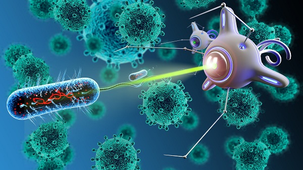
Nano robot 3D render. Medical concept future.
Nanomedicine:
Nanomedicine is already a thriving area of practice. The term refers “to the use of materials at the nanoscale to diagnose and treat disease. Some researchers define nanomedicine as encompassing any medical products using nanomaterials smaller than 1,000 nanometers. Others more narrowly use the term to refer to injectable drugs using nanoparticles smaller than 200 nanometers.”
The means of transporting nanomedicine can be done by nanobots. There was a movie made years back called Fantastic Voyage. The plot was that a scientist is nearly assassinated and in order to save him, a submarine was shrunken to microscopic size and injected into his bloodstream with a small crew. My former neighbor, the late Dr. Aaron Josephson, of Michael Resse Hospital in Chicago was an advisor to the movie. Although we cannot shrink a crew, we can use nanobots for medical purposes, especially drug delivery. “Nanobots are robots that can be used very effectively for drug delivery. Normally, drugs work through the entire body before they reach the disease-affected area. Using nanotechnology, the drug can be targeted to a precise location which would make the drug much more effective and reduce the chances of possible side effect.”
Nanotechnologies have created significantly enhanced imaging and diagnostic tools to help enable earlier diagnosis, treatments, and therapeutics. Nanotech is being used to enhance bone and neural tissue engineering. It is also a component involved in the successful implantation of bionic eyes, kidneys, hearts, and other body parts. Advanced pliable materials such as plastics, ceramics, metals, and graphene are also being used for prosthetics for medical applications.
Nanoparticles are also playing an amazing role in the creation of gene sequencing technologies, drug delivery, including vaccines. Nanopore technology has become increasingly important in the field of life science and biomedical research, including genomics. The nanopore technology embeds nano-scale holes in a thin membrane and measures the electrochemical signal to investigate biomacromolecules.
3-D Printing manufacturing with nanoparticles also can be used for medicine via bioprinting. Three-dimensional (3-D) Bioprinting means creating living tissues, such as blood vessels, bones, heart or skin, via the additive manufacturing technology.
In a recent interview, Erik Gatenholm, CEO of CELLINK, estimated that “we will see fully functioning organs within the next decade or so.” Gatenholm added, “scientists have been able to bio print hearts, lungs, kidneys, skin, corneas and more throughout the last 5 years and are currently working towards developing full functioning organs.”
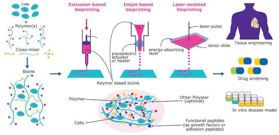
3d-bioprinting-tissue-organs.
Nanotech is also used as a means of prevention against current and future pandemics. Dr. Mark Banash (PhD, Princeton University; BS University of Pennsylvania), previously mentioned above is considered a leading authority in both nanomaterials and nanotechnology applied to manufacturing and industrial scale applications. He’s the CTO of JP Industries International and has been leading efforts developing several nanotechnology-based solutions to a wide range of healthcare problems, including those involving personal protection and security with solutions that kills viruses, bacteria, and fungal contaminations on surfaces. Mark and his team also uses nanotech to increase the efficacy and efficiency of PPE protective coatings in for individuals during pandemics and for environmental uses including safer water treatment.
We are already going through biomedical changes like nanotechnology implants that will challenge our notion of technology and people. Nanotech is exploring the edge of science. One such development includes an injectable biosensor that might one day be able to read your thoughts or let you communicate with nothing but your mind.
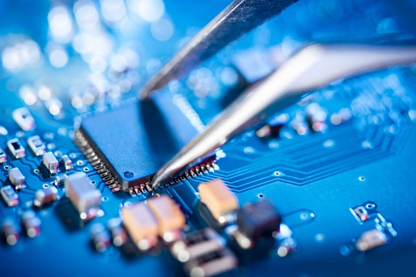
Electronic technician holding tweezers and assemblin a circuit board.
Device Engineering (electronics, wearables):
Nano technologies have led to advancements in device engineering that feature more compact and capable computers. Our smartphones exemplify how far we have come in device engineering via microprocessors and chips used in electrical circuitry. Your smartphone has more computing capabilities that the massive computers used to send astronauts to the moon during the Apollo Space Program.
Nanotechnology is used in electronic devices such as laptops, computers, cell phones, TVs, and electronic sensing and communications which is used in most transportation including, airplanes, trains, and autonomous vehicles. It is also integral to satellites that continually monitor the Earth for environmental, and security purposes.
The field of smart devices and robotics has been transformed by nanotech because of several factors. “The appeal of nano-technology for smart devices is broad, with many consumers and developers with different benefits. The appeal comes down to a number of important factors:
1. nanotechnology shrinks the device to a convenient size for the home
2. it increases the performance and intelligence capabilities
3. it allows for new functions within familiar tech for increased potential
4. it provides new surfaces and nano-coatings for strength and high performance
5. it provides safe nano-particles to improve cleanliness and hygiene.”
An extensive research resource for evolving nanoelectronics applications is summarized below in an article “Nanoelectronics; Nanotechnology in Electronics:
– “Researchers at the University of Michigan have demonstrated a technique to grow single layers of hexagonal boron nitride on graphene. The boron nitride can be used as an insulator, so this technique may lead to wafer level sheets of very thin graphene insulated by very thin boron nitride.
– Researchers at Harvard have used nano fabrication techniques to build a laser on a lithium niobate chip, to be used in lithium niobate photonic circuits.
– Researchers at NIST have demonstrated an LED build with zinc oxide nanostructures called fins which generates much higher light output than existing designs of similar size. The researchers also found that raising the current caused the structure to generate laser light.
– Researchers at the Royal Melbourne Institute of Technology have demonstrated atomically-thin indium-tin oxide sheets that may make touchscreens that are cost less to manufacture and well as being flexible and consumes less power.
– Cadmium selenide nanocrystals deposited on plastic sheets have been shown to form flexible electronic circuits. Researchers are aiming for a combination of flexibility, a simple fabrication process and low power requirements.
– Integrating silicon nanophotonics components into CMOS integrated circuits. This optical technique is intended to provide higher speed data transmission between integrated circuits than is possible with electrical signals.
– Researchers at UC Berkeley have demonstrated a low power method to use nanomagnets as switches, like transistors, in electrical circuits. Their method might lead to electrical circuits with much lower power consumption than transistor based circuits.
– Researchers at GeorgiaTech, the University of Tokyo and Microsoft Research have developed a method to print prototype circuit boards using standard inkjet printers. Silver nanoparticle ink was used to form the conductive lines needed in circuit boards.
– Researchers at Caltech have demonstrated a laser that uses a nanopatterned silicon surface that helps produce the light with much tighter frequency control than previously achieved. This may allow much higher data rates for information transmission over fiber optics.
– Building transistors from carbon nanotubes to enable minimum transistor dimensions of a few nanometers and developing techniques to manufacture integrated circuits built with nanotube transistors.
– Researchers at Stanford University have demonstrated a method to make functioning integrated circuits using carbon nanotubes. In order to make the circuit work they developed methods to remove metallic nanotubes, leaving only semiconducting nanotubes, as well as an algorithm to deal with misaligned nanotubes. The demonstration circuit they fabricated in the university labs contains 178 functioning transistors.
– Developing a lead free solder reliable enough for space missions and other high stress environments using copper nanoparticles.
– Using electrodes made from nanowires that would enable flat panel displays to be flexible as well as thinner than current flat panel displays.
– Using semiconductor nanowires to build transistors and integrated circuits.
– Transistors built in single atom thick graphene film to enable very high speed transistors.
– Researchers have developed an interesting method of forming PN junctions, a key component of transistors, in graphene. They patterned the p and n regions in the substrate. When the graphene film was applied to the substrate electrons were either added or taken from the graphene, depending upon the doping of the substrate. The researchers believe that this method reduces the disruption of the graphene lattice that can occur with other methods.
– Combining gold nanoparticles with organic molecules to create a transistor known as a NOMFET (Nanoparticle Organic Memory Field-Effect Transistor).
– Using carbon nanotubes to direct electrons to illuminate pixels, resulting in a lightweight, millimeter thick "nanoemmissive" display panel.
Making integrated circuits with features that can be measured in nanometers (nm), such as the process that allows the production of integrated circuits with 22 nm wide transistor gates.
– Using nanosized magnetic rings to make Magnetoresistive Random Access Memory (MRAM).
– Researchers have developed lower power, higher density method using nanoscale magnets called magnetoelectric random access memory (MeRAM).
– Developing molecular-sized transistors which may allow us to shrink the width of transistor gates to approximately one nm which will significantly increase transistor density in integrated circuits.
– Using self-aligning nanostructures to manufacture nanoscale integrated circuits.
– Using nanowires to build transistors without p-n junctions.
– Using buckyballs to build dense, low power memory devices.
– Using magnetic quantum dots in spintronic semiconductor devices. Spintronic devices are expected to be significantly higher density and lower power consumption because they measure the spin of electronics to determine a 1 or 0, rather than measuring groups of electronics as done in current semiconductor devices.
– Using nanowires made of an alloy of iron and nickel to create dense memory devices. By applying a current magnetized sections along the length of the wire. As the magnetized sections move along the wire, the data is read by a stationary sensor. This method is called race track memory.
– Using silver nanowires embedded in a polymer to make conductive layers that can flex, without damaging the conductor.
– IMEC and Nantero are developing a memory chip that uses carbon nanotubes. This memory is labeled NRAM for Nanotube-Based Nonvolatile Random Access Memory and is intended to be used in place of high density Flash memory chips.
– Researcher have developed an organic nanoglue that forms a nanometer thick film between a computer chip and a heat sink. They report that using this nanoglue significantly increases the thermal conductance between the computer chip and the heat sink, which could help keep computer chips and other components cool.
– Researchers at GeorgiaTech, the University of Tokyo and Microsoft Research have developed a method to print prototype circuit boards using standard inkjet printers. Silver nanoparticle ink was used to form the conductive lines needed in circuit boards.”

Young female doctor looking at hologram screen. Electronic medical record. Smart glasses. Medical technology concept.
Wearables:
A major area of nanotech device engineering is focused on wearables. These include flexible electronics, wrist bands, rings, glasses, ear pods as well as contact lenses that are attachable, wearable, and embedded. The trend of wearable sensors is an emerging one with limitless possibilities for performance, security, and health.
Wearables are being studied and used to monitor health at government run health facilities and can provide real-time biomarker tracking. Wearable technology is helping protect those in public safety. Firefighters can ingest sensors and data-transmitting pills to track their heart rate, which will then send an alert to pull a firefighter out of disaster before cardiac arrest or heat stress sets in. High-tech wearable headsets allow military personnel to live-stream 3-D maps of battlefields and different drone feeds, among other features.
The question is no longer when wearable tech will be available, but how fast, these biometric technologies will extend human /computer interface capabilities and how ingrained in our daily lives that these technologies will become. There are futurists who think that eventually many biological functions will be replaced by nano components operating in bionic machines.
As a cybersecurity advocate, it should be noted that just like mobile devices, wearables can be hacked or infected with malware. Developing protocols for monitoring, testing, and securing critical citizen information will be necessary, especially for public use. In an increasingly connected world, privacy and security will be paramount.
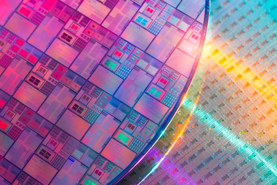
Silicon Wafers and Microcircuits with Automation system control application
Nanotechnologies are fundamental to those technology breakthroughs as we witness and experience the change. According to experts, the global market for Nanotechnology is projected to reach a size of US $70.7 Billion by 2026.
The technological transformation we are experiencing is happening at an exponential rate of change. So fast, in fact, that I must continually update a course called “Disruptive Technologies and Organizational Management” that I created and teach at Georgetown University’s Graduate Cybersecurity Risk Management program. There is hardly a day that goes by when there isn’t an article on an innovative technology breakthrough or discovery.
We may not be able to visibly see most of the nano components, but they are certainly impacting our future in a grand way.
Read the original article on Forbes.