
Excitons are bound electron-hole pairs that can interact with electrical charges, spins, and phonons. This range of interactions indicates that excitons could be herald a new wave of devices based on nanoscale photonics and optoelectronics.
With this promise in mind, Rasmus Godiksen set forth to explore the potential of excitons in ultra-thin semiconductors such as molybdenum disulfide (MoS2) and tungsten disulfide (WS2). The semiconductors are so thin that can be approximated as 2D materials. So, in effect, Godiksen wanted to study excitons in 2D materials.
Sensitivity
First off, Godiksen and his collaborators showed that the 2D excitons are very sensitive to their nanoscopic environment. Using photoluminescence (PL) imaging techniques, he measured fluorescence fluctuations due to charge transfer to the semiconductor. Such fluctuations are spatially correlated over tens of micrometers in WS2 monolayers on metal films.
Due to charge fluctuations from trap states (which are states that trap excited carriers such as electrons, holes, and excitons), they follow power-law statistics with simultaneous changes in emission intensity, lifetime, and exciton-trion ratios. Power-law statistics in an indicator of trapping and de-trapping of excitons, so this provides evidence of trapped states.
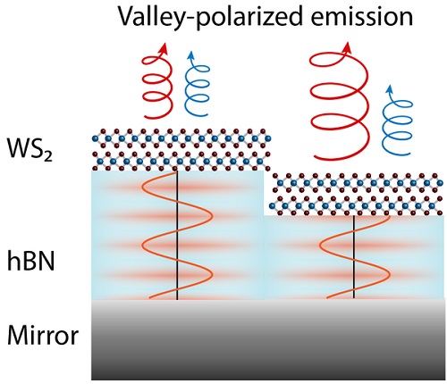
Valley degree of freedom
Excitons in WS2 also have a degree of freedom with regards to valleys, which couples spin polarization to momentum direction. Valleys in the band structure can be explored using circularly polarized light. Exciting or detecting an exciton in one valley can be used in information technologies, for example.
To explain the contrast in spin-valley polarization in a few layers of WS2 and tungsten diselenide (WSe2), Godiksen used layer- and temperature-dependent circularly polarized PL measurements. This related their contrasting polarizations to a different momentum of their conduction band minima.
The overall spin-valley dynamics are governed by the exciton and valley lifetimes. Valley polarized emission is determined by competing lifetimes – the exciton lifetime and the valley lifetime. By decreasing the exciton lifetime, it’s possible to increase valley polarized emission. This is because excitons recombine and emit light faster than they scatter to the other available valleys.
By changing the distance of a WS2 bilayer to a mirror, the excitation enhancement increases exciton-exciton annihilation resulting in higher polarization.
Silion nanoresonators
Finally, Godiksen studied the use of silicon nanoantenna to further enhance the interaction of circularly polarized light with valley-polarized excitons. He shows that crystalline silicon nanodisks preserve the circular polarization of light in the near field as required for additional enhancement of valley-polarized emission.
Godiksen’s results advance the understanding of the interaction of excitons with charges, spins, and photons with implications for a range of nanophotonic devices using atomically thin semiconductors.
Single-photon sources are interesting for quantum computing, molecular sensors could increase sensitivity down to the single molecule level, and valleytronic devices could pave the way for a new generation of electronic devices based on valley polarization.
After his PhD research at TU/e, Godiksen will take up a position as an optical design engineer at Ibsen Photonics in Denmark.
Title of PhD thesis: “Atomically thin semiconductors for nanophotonics”. Supervisors: Jaime Rivas Gómez and Alberto Curto.
Read the original article on Eindhoven University of Technology (TU/e).