In 2004, researchers from the University of Manchester used adhesive tape to pull sheets of single carbon atoms away from graphite to make graphene—a material that is 1000 times thinner than human hair yet stronger than steel. This ground-breaking exfoliation technique paved the way for the development of a wide range of two-dimensional materials with distinct electrical and physical characteristics for the next generation of electronic devices.
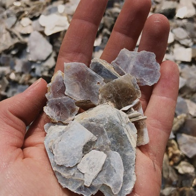
One such material of interest has been muscovite mica (MuM). These minerals have the general formula KAl2(AlSi3O10) (F, OH)2 and have a layered structure consisting of aluminum (Al), potassium (K), and silicon (Si). Like graphene, MuM has gained attention as an ultra-flat substrate for building flexible electronic devices. Unlike graphene, however, MuM is an insulator.
Muscovite mica (MuM) is a layered mineral commonly used as an insulator. In a new study, researchers observed that, when thinned down to a few molecule layers, MuM acts more like a semiconductor with a thickness-dependent conductivity.
However, the electrical properties of MuM are not altogether clear. In particular, the properties of single and few-molecule-layer thick MuMs are not clearly understood. This is because in all the studies that have probed the electrical properties of MuM so far, the conductivity has been dominated by a quantum phenomenon called “tunneling.” This has made it difficult to understand the conductive nature of thin MuM.
In a recent study published in the journal Physical Review Applied, Professor Muralidhar Miryala from Shibaura Institute of Technology (SIT), Japan, Professors M. S. Ramachandra Rao, Ananth Krishnan and Mr. Ankit Arora, a PhD student, from Indian Institute of Technology Madras, India, have now observed a semiconducting behavior in thin MuM flakes, characterized by an electrical conductivity that is 1000 times larger than that of thick MuM. “Mica has been one of the most popular electrical insulators used in industries for decades. However, this semiconductor-like behavior has not been reported earlier,” say Prof. Miryala and Prof. Rao.
In their study, the researchers exfoliated thin MuM flakes of varying thickness onto silicon (SiO2/Si) substrates and, to avoid tunneling, maintained a separation of 1 µm between the contact electrodes. On measuring the electrical conductivity, they noticed that the transition to a conducting state occurred gradually as the flakes were thinned down to fewer layers. They found that for MuM flakes below 20 nm, the current depended on the thickness, becoming 1000 times larger for a 10 nm thick MuM (5 layers thick) compared to that in 20 nm MuM.
To make sense of this result, the researchers fitted the experimental conductivity data to a theoretical model called the “hopping conduction model,” which suggested that the observed conductance is due to an increase in the conduction band carrier density with the reduction in thickness. Put simply, as the thickness of MuM flakes is reduced, the energy required to move electrons from the solid bulk to the surface decreases, allowing the electrons easier passage into the “conduction band,” where they can freely move to conduct electricity. As to why the carrier density increases, the researchers attributed it to the effects of surface doping (impurity addition) contributions from K+ ions and relaxation of the MuM crystal structure.
The significance of this finding is that thin exfoliated sheets of MuM have a band structure similar to that of wide bandgap semiconductors. This, combined with its exceptional chemical stability, makes thin MuM flakes an ideal material for two-dimensional electronic devices that are both flexible and durable. “MuM is known for its exceptional stability in harsh environments, such as those characterized by high temperatures, pressures, and electrical stress. The semiconductor-like behavior observed in our study indicates that MuM has the potential to pave the way for the development of robust electronics,” says Prof. Miryala.
There is certainly more to mica than meets the eye!
Read the original article on Shibaura Institute of Technology.