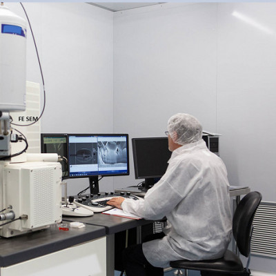
Cutting intricate patterns as small as several billionths of a meter deep and wide, the focused ion beam (FIB) is an essential tool for deconstructing and imaging tiny industrial parts to ensure they were fabricated correctly. When a beam of ions, typically of the heavy metal gallium, bombards the material to be machined, the ions eject atoms from the surface—a process known as milling—to sculpt the workpiece.
Beyond its traditional uses in the semiconductor industry, the FIB has also become a critical tool for fabricating prototypes of complex three-dimensional devices, ranging from lenses that focus light to conduits that channel fluid. Researchers also use the FIB to dissect biological and material samples to image their internal structure.
However, the FIB process has been limited by a trade-off between high speed and fine resolution. On the one hand, increasing the ion current allows a FIB to cut into the workpiece deeper and faster. On the other hand, the increased current carries a larger number of positively charged ions, which electrically repel each other and defocus the beam. A larger, diffuse beam, which can be about 100 nanometers in diameter or 10 times wider than a typical narrow beam, not only limits the ability to fabricate fine patterns but can also damage the workpiece at the perimeter of the milled region. As a result, the FIB has not been the process of choice for those trying to machine many tiny parts in a hurry.
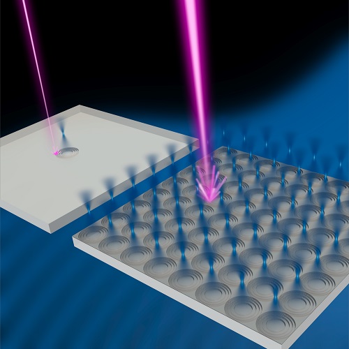
NIST researchers have demonstrated that a focused ion beam (FIB) can fabricate microscopic devices with fine resolution and without sacrificing high speed. Left: The conventional FIB process requires a narrow, low-current ion beam to fabricate a miniature version of a lighthouse lens in silica glass with fine resolution. Because the beam has a low current of ions, the method is time consuming. Right: Placing a protective layer of chromium oxide over the silica glass enables machinists to use a much higher-current ion beam, allowing them to fabricate the same lenses 75 times faster.
Now researchers at the National Institute of Standards and Technology (NIST) have discovered that a masking process can virtually eliminate this trade-off, enabling a FIB to machine at high current (and therefore high speed) without sacrificing fine resolution. The finding could dramatically expand the utility of FIBs, not only for researchers fabricating prototypes and preparing samples, but also for manufacturers in the semiconductor industry who need rapid analysis, repair, or customization of structures and devices.
“In both research and in production, the need for speed is real,” said NIST researcher Andrew C. Madison.
Madison and his colleagues at NIST, including Samuel M. Stavis and a collaborator from the University of Maryland NanoCenter in College Park, compared the efficiency of two processes for achieving fine resolution with a FIB. In one process, fabricators simply use a FIB with a low-current, narrow beam to slowly but carefully sculpt the workpiece—similar to the way a painter with a fine brush painstakingly creates sharp details.
The other method employs a higher-current, wider beam along with a mask, or thin film, deposited on the workpiece. The central, most intense region of the ion beam penetrates the mask and blasts the underlying material to form the pattern. The outer, less intense region of the beam is blocked by the mask, protecting the sample from damage at the edges of the pattern.
The masking process is similar to that of a painter who puts masking tape around the edges of a wide area and then uses a roller rather than a fine brush to rapidly paint the wide area while still achieving sharp edges.
The NIST team determined that beams of much higher-than-normal current can be used without compromising the fine details of the pattern. Previous studies examining masking focused only on improving resolution without considering the effect of the mask on the speed of fabrication. Whereas the finer resolution provided by the masking process was plainly evident from these studies, the NIST researchers discovered a much greater improvement in speed.
The researchers used chromium oxide as a mask, studying its material properties and how gallium ions from the FIB interacted with it. They then employed a high-current, wide beam to blast a checkerboard test pattern into silica glass. They found that the masking process not only provided similarly fine resolution to the unmasked, narrow-beam process, but also milled the sample much faster due to the higher beam current.
Encouraged by the result, the team then used the mask with a wide, high-current beam to machine compact Fresnel lenses—microscopic versions of lighthouse lenses—which are useful in optical devices ranging from solar cells to atom traps. Even though the high-current beam was about 10 times wider than the low-current beam, the method yielded lenses that performed the same to within an uncertainty of 1%. In this way, the researchers confirmed that they could fabricate similar lenses 75 times faster than they could using the conventional process. “If time is money, then our process enables a big sale on small lenses—75 for the price of one,” said Stavis. “Want to mill fast? Get you a mask,” he added. The team reported their findings in Advanced Functional Materials on August 21, 2022.
Read the original article on National Institute of Standards and Technology (NIST).