
Frank Holzenburg, an artist with tens of thousands of followers across his social networking accounts, has attracted attention for his life-like drawings that are smaller than a fingernail. Recently, a method to draw data in an area smaller than 10 nanometers (nm; 1 nm = 1 billionth of a meter) – like drawing a small picture on paper – has been proposed.
A joint research team led by Professor Daesu Lee (Department of Physics) of POSTECH, Professor Se Young Park (Department of Physics) at Soongsil University, and Dr. Ji Hye Lee (Department of Physics and Astronomy) of Seoul National University has proposed a method for densely storing data by ‘poking’ with a sharp probe. This method utilizes a material in the metastable*1 state, whose properties change easily even with slight stimulation.
A thin film of metastable ferroelectric*2 calcium titanate (CaTiO3) enables the polarization*3 switching of a material even with a slight pressure of a probe: A very weak force of 100 nanonewtons (nN) is more than enough. The joint research team succeeded in making the width of the polarization path smaller than 10 nm by using this force and found the way to dramatically increase the capacity of data storage. This is because the smaller the size of the path, the more data the single material can store.
The data storage capacity increased by up to 1 terabit (Tbit)/cm as a result of drawing the data storage area using a probe on the thin film. This result is 10 times greater than that of a previous study (0.11Tbit/cm²) which suggested a probe-based storage method using another material. Unlike the data storage method that uses electric fields, this probe method only requires a very small force, so the burden on the device is also small.
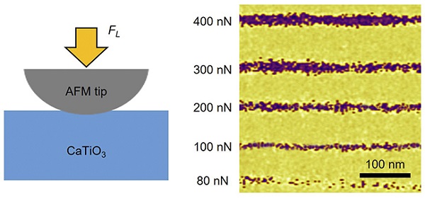
Left: Data storage using probe force. Right: Data storage area drawn with a width of 10 nm or less.
The results from the study are drawing attention as they have proved that materials achieve higher performance in an unstable metastable state. The findings are anticipated to be applicable in the next-generation electronic devices with improved integration and efficiency in the future.
Recently published in Physical Review Letters, one of the most authoritative journals in the field of physics, this study was supported by the Institute for Basic Science, and by the Research Center Program, the Basic Science Research Institute Fund, and the Key Research Institutes in Universities program of the National Research Foundation of Korea.
Read the original article on Pohang University of Science and Technology (POSTECH).