Spark plasma sintering (SPS) is a process that uses high-pressure and pulsed electric current to turn powders into dense solids. In a recent study, a team of researchers used SPS to prepare bulk magnesium diboride with a density that reached 95% of the theoretical limit for the material. The highly dense material also exhibited excellent superconducting properties, holding much promise for its applications in superconducting motors, generators, and transport.
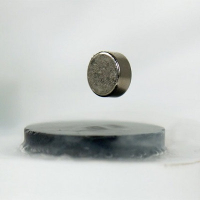
From superfast magnetic levitation trains and computer chips to magnetic resonance imaging (MRI) machines and particle accelerators, superconductors are electrifying various aspects of our life. Superconductivity is an interesting property that allows materials to transfer moving charges without any resistance, below a certain critical point. This implies that superconducting materials can transfer electrical energy in a highly efficient manner without loss in the form of heat, unlike many conventional conductors.
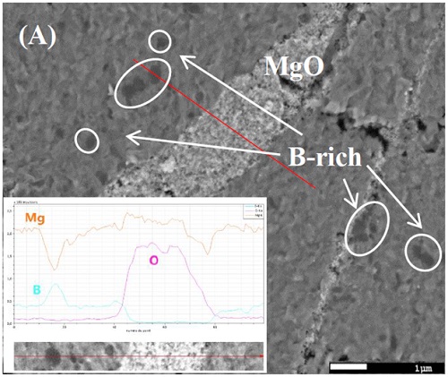
Title: An SEM micrograph of MgB2, a superconductor, prepared at SIT, with different regions mapped.
Caption: Scientists at SIT and University of Normandie developed bulk MgB2 with promising superconductivity. This picture shows unreacted magnesium oxide and boron in the matrix of MgB2, and the inset shows energy dispersive x-ray spectroscopy curves for boron, oxygen, and magnesium.
Almost two decades ago scientists discovered superconductivity in a new material—magnesium diboride, or MgB2. There has been a resurgence in the of popularity MgB2 due to its low cost, superior superconducting abilities, high critical current density (which means that compared to other materials, MgB2 remains a semiconductor even when larger amounts of electric current is passed through it), and trapped magnetic fields arising from strong pinning of the vortices—which are cylindrical current loops or tubes of magnetic flux that penetrate a superconductor. The intermetallic MgB2 also allows adjustability of its properties. For instance, the critical current density values (Jc) of MgB2 can be improved by decreasing the grain size and increasing the number of grain boundaries. Such adjustability is not observed in conventional layered superconductors.
To widen the applications of MgB2, however, there is a need to simplify the method of its preparation. Recently, a team of researchers embarked on a journey to do so. They fabricated a novel bulk MgB2 via a process called spark plasma sintering (SPS). In their recent article, published first on 27 July 2022 in Nanomaterials, Prof. Muralidhar Miryala from Shibaura Institute of Technology (SIT), Japan, who led the group, explains “Spark plasma sintering (SPS) is a very interesting technique—it is a rapid consolidation method, where powder is turned into a dense solid. The heat source in this procedure is not external but is an electric current that flows across the die, causing the powder to sinter into a bulk material. The sintering kinetics can be understood and controlled better with SPS. Unlike other similar techniques, it allows grain growth control. What’s more, it also has a shorter processing time!”
Prof. Miryala and Prof. Jacques G. Noudem (from the University of Normandie, France) had used this unconventional method to prepare bulk samples of MgB2. The resultant material had excellent superconducting properties and a density that reached 95% of what was theoretically predicted for the material. The study team included Prof. Pierre Bernstein and Yiteng Xing, who is a double degree Ph.D. student at SIT and the University of Normandie.
To synthesize the bulk MgB2, the team loaded two powders—magnesium and amorphous boron—into a tungsten carbide (WC) mold and sintered them using SPS at different temperatures ranging from 500–750°C, and pressure ranging from 260–300 megapascal (MPa), then cooled the formed material. The total processing time was about 100 minutes. The team then analyzed the density and the structural properties of the prepared material, using various imaging and testing methods.
Their experiments revealed that the material had a very high density of 2.46 g/cm3 and a high packing factor of 95% (indicating that the atoms in the bulk material were situated very close to each other). It also showed the presence of nano-grains and a large number of grain boundaries. Moreover, it did not exhibit Mg-depleted phases like MgB4. Electromagnetic characterization of the material showed that it exhibited an extremely high Jc of up to 6.75 105 ampere/cm2 at about -253°C. This means that even at that high a current density, the bulk MgB2 made by the team would act as a superconductor. “Its Jc was quite remarkable for pure, undoped MgB2,” commented Prof. Miryala.
Curious as to how the material exhibited such excellent properties, the team dug deeper. They concluded that the prepared MgB2’s superconducting properties were due to its high density, excellent grain connectivity (due to no Mg-depleted phases), and the strong pinning of vortices availed by the presence of nano-grains and grain boundaries.
This study provided a new way to improve the properties of superconducting materials like MgB2. Given this material’s high Jc, it can be used in liquid hydrogen-cooled technology. It is also emerging as a promising candidate for liquid hydrogen-based transportation, storage, and fuel systems. “Global warming is one of the major threats humanity is facing today and shifting to a renewable energy economy is one of the most effective solutions to this problem. Given the material’s potential use in liquid hydrogen systems and its excellent structural and superconducting properties, our work is a positive step towards the realization of greener technology,” concludes Prof. Miryala.
A hope for a sustainable and greener tomorrow indeed!
Read the original article on Shibaura Institute of Technology.