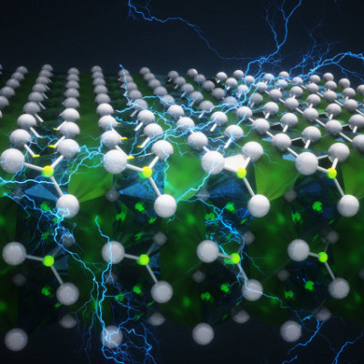
"Ferroelectric materials are all around us, most commonly within capacitors in our cellphones, televisions and any other electronic device," said Salvador Barraza-Lopez, associate professor of physics and theory lead for the team.
"Ferroelectric materials possess an intrinsic electric dipole moment that can be switched by electric fields," he added. "When ferroelectric materials are warmed up, their intrinsic dipole moment becomes quenched until it becomes zero at a so-called critical temperature. At even higher temperatures, those materials are called paraelectric."
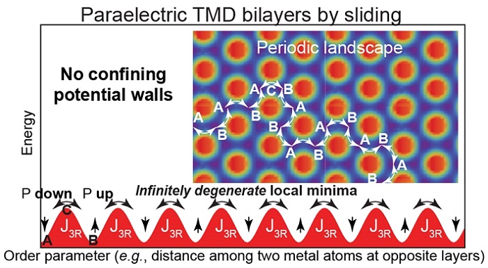
Energy cost of moving one atomic layer onto another.
Barraza-Lopez said there is an ongoing effort to deploy ferroelectric materials that are a few atoms thick, and a team at Columbia University demonstrated a paraelectric transition on materials known as transition metal dichalcogenide bilayers earlier this year.
"They did not say, however, how atoms must reacommodate to achieve such paraelectric configuration," he said.
So Barraza-Lopez led a collaboration among theory groups at the U of A and Montana State University to help understand how atoms arrange as they turn from a ferroelectric configuration onto a paraelectric one, and what they found turned out to be rather unusual.
"Typically, a paraelectric configuration is one in which atoms turn onto a structure with a higher symmetry," Barraza-Lopez said. "For example, a ferroelectric material with a rectangular structure turns into a paraelectric square."
For the materials being studied, however, the team was unable to find a paraelectric phase.
"What we observed instead was that the putative paraelectric behavior is rather a time average of a ferroelectric configurations swapping among two polarization states as time goes by," said Barraza-Lopez, adding that these results were recently published in the journal Nano Letters.
Barraza-Lopez said this discovery was made possible by financial support from the MonArk NSF Quantum Foundry, a center whose mission is to understand the behavior of two-dimensional materials, and their possible applications.
Collaborators included Joseph Roll, an undergraduate student in physics, and Shiva Poudel, a postdoctoral associate in Barraza-Lopez's group, as well as Juan Marmolejo-Tejada and Martin Mosquera from the Department of Chemistry and Biochemistry at Montana State University.
Read the original article on University of Arkansas.