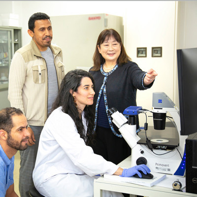
Semiconductors are foundational components of modern energy, communication, and myriad other technologies. Research on tailoring the underlying nanostructure of semiconductors for optimizing device performance has been ongoing for decades. Now, in a study recently published in Scientific Reports, researchers from the University of Tsukuba and collaborating partner UNISOKU Co., LTD., have facilitated technology development—easy-to-use, time-resolved scanning tunneling microscopy (STM)—for measuring the movement of electrons in nanostructures at high temporal and spatial resolution, in a manner that will be invaluable for optimizing nanostructure performance.
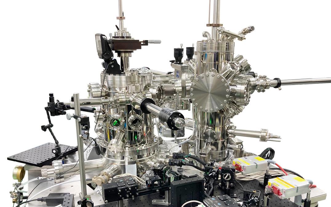
Current flow through semiconductors, and thus their performance, depends on the dynamics of charge carriers. These dynamics can be extremely fast. For example, their dynamics can be more than 10 billion times faster than the millisecond range of the blink of an eye. Optical pump-probe (OPP) STM is the present state-of-the-art, essential method for measuring and imaging such dynamics in semiconductors. However, present means of measuring and imaging systems are too complicated for non-experts. Special techniques are needed for data acquisition and interpretation. Therefore, ease of operation and ease of use are what the researchers sought to address in this study.
"OPP STM is an essential method for measuring photo-induced charge carrier dynamics in nanostructures, but requires technical advances to meet ultrafast observation needs," explains Professor Hidemi Shigekawa, senior author. "Our updates to OPP STM enabled study of ultrafast carrier dynamics in a common semiconducting material."
The researchers report particularly noteworthy techniques that helped optimize the performance of the developed system. They introduced a mechanism to electrically control the laser oscillation as well as the delay time between the pump and probe lights, and constructed a stable optical system. They used this user-friendly system to measure ultrafast charge carrier dynamics on gallium arsenide surfaces. They also succeeded in applying their technique to correlate defects such as step edges and terraces to charge carrier dynamics. This correlation was enabled in part by the high stability of the imaging, meaning that it was conducted on a stabilized light spot position over 16 hours.
"Our work will be invaluable in fields such as ultrafast optical communication technologies and photocatalysis," say the researchers. "Relating the underlying nanostructure of materials to corresponding photo-electrical properties by this user-friendly method will provide fundamental knowledge that's necessary for improving semiconductor device functionality."
This work succeeded in expanding the utility of OPP STM for studying nanostructure-function relationships of semiconducting materials such as gallium arsenide and low-dimensional materials. The researchers' straightforward experimental design will help researchers in various fields improve the photo-electrical performance of, for example, integrated circuits and light-emitting diodes for ultrafast optical communication technologies. The performance of time-resolved OPP STM can be further improved by optimizing the wavelength and temporal width of the pulsed laser; substantial developments are expected.
Read the original article on University of Tsukuba.