2023-04-24
Visited : 1435
A team of Brown University researchers created a solution to a nanoscale resolution challenge that has for decades limited the study of materials that could lead to more energy efficient semiconductors and electronics.
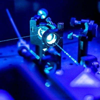
With a new microscopy technique that uses blue light to measure electrons in semiconductors and other nanoscale materials, a team of Brown University researchers is opening a new realm of possibilities in the study of these critical components, which can help power devices like mobile phones and laptops.
The findings are a first in nanoscale imaging and provide a workaround to a longstanding problem that has greatly limited the study of key phenomena in a wide variety of materials that could one day lead to more energy-efficient semiconductors and electronics. The work published in Light: Science & Applications.
“There is a lot of interest these days in studying materials with nanoscale resolution using optics,” said Daniel Mittleman, a professor in Brown’s School of Engineering and author of the paper describing the work. “As the wavelength gets shorter, this becomes a lot harder to implement. As a result, nobody had ever done it with blue light until now.”
Typically, when researchers use optics like lasers to study nanoscale materials, they use light that emits long wavelengths such as red light or infrared. The method the researchers looked at in the study is called scattering-type scanning near-field microscopy (s-SNOM). It involves scattering light from a sharpened tip that is only a few tens of nanometers across. The tip hovers just above the sample material to be imaged. When that sample is illuminated with optical light, the light scatters and a portion of the scattered light is left with information about the nano-sized region of the sample directly beneath the tip. The researchers analyze that scattered radiation to extract information about this small volume of material.
The technique has been at the foundation of many technological advances, but it hits a wall when it comes to using light with a much shorter wavelength, like blue light. This means that using blue light, which is better suited for studying certain materials for which red light is ineffective, to gain new insights from already well-studied semiconductors has been out of reach since the 1990s when the technique was invented.
In the new study, the researchers from Brown present how they got around this roadblock to perform what’s believed to be the first ever experimental demonstration of s-SNOM using blue light instead of red.
For the experiment, the researchers used the blue light to get measurements from a silicon sample that cannot be obtained using red light. The measurements provided a valuable proof-of-concept about the use of shorter wavelengths to study materials on the nanoscale.
“We were able to compare these new measurements to what one might expect to see from silicon, and the match was very good,” Mittleman said. “It confirms that our measurement works and that we understand how to interpret the results. Now we can start studying all these materials in a way that we couldn't before.”
To conduct the experiment, the researchers had to get creative. Essentially, they decided to make things easier by making them more complicated. With the typical technique, for instance, blue light is hard to use because its wavelength is so short, meaning that it is more challenging to focus over the right spot near the metal tip. If not aligned just right, the measurement won’t work. With the red light, this focusing condition is more relaxed, making it easier to align the optics in order to extract the scattered light efficiently.
With those challenges in mind, the researchers used the blue light to not only illuminate the sample so that the light scatters, but also to produce a burst of terahertz radiation from the sample. The radiation carries important information about the sample’s electrical properties. While the solution adds an extra step and increases the amount of data the scientists have to analyze, it eliminates the need to be as precise in how they align the tip over the sample. The key here is that because the terahertz radiation has a much longer wavelength, it is much more easily aligned.
“It still has to be really close, but it doesn’t have to be as close,” Mittleman said. “When you hit it with the light, you’ll still be able to get information in the terahertz.”
The researchers are excited to see what comes next in terms of new information and discoveries the method leads to, such better insights into semiconductors used to produce blue LED technology. Mittleman is currently developing plans to use blue light to analyze materials researchers haven’t been able to before.
Read the original article on Brown University.