The prototype device demonstrates the potential of this emerging photovoltaic technology to overcome key limits associated with traditional silicon solar cells, while also offering a lower manufacturing cost.
“Further improvements in the efficiency of solar cells are crucial for the ongoing decarbonization of our economy,” says U of T Engineering Professor Ted Sargent (ECE), who recently joined the Department of Chemistry and the Department of Electrical and Computer Engineering at Northwestern University.
“While silicon solar cells have undergone impressive advances in recent years, there are inherent limitations to their efficiency and cost, arising from material properties. Perovskite technology can overcome these limitations, but until now, it had performed below its full potential. Our latest study identifies a key reason for this and points a way forward.”
Traditional solar cells are made from wafers of extremely high-purity silicon, which is energetically costly to produce. By contrast, perovskite solar cells are built from nano-sized crystals that can be dispersed into a liquid and spin-coated onto a surface using low-cost, well-established techniques.
Another advantage of perovskites is that by adjusting the thickness and chemical composition of the crystal films, manufacturers can selectively ‘tune’ the wavelengths of light that get absorbed and converted into electricity, whereas silicon always absorbs the same part of the solar spectrum.
In a new paper published today in Nature, the international team of researchers used two different layers of perovskite, each tuned to a different part of the solar spectrum, to produce what is known as a tandem solar cell.
“In our cell, the top perovskite layer has a wider band gap, which absorbs well in the ultraviolet part of the spectrum, as well as some visible light,” says Chongwen Li, a postdoctoral researcher in Sargent’s lab and one of five co-lead authors on the new paper.
“The bottom layer has a narrow band gap, which is tuned more toward the infrared part of the spectrum. Between the two, we cover more of the spectrum than would be possible with silicon.”
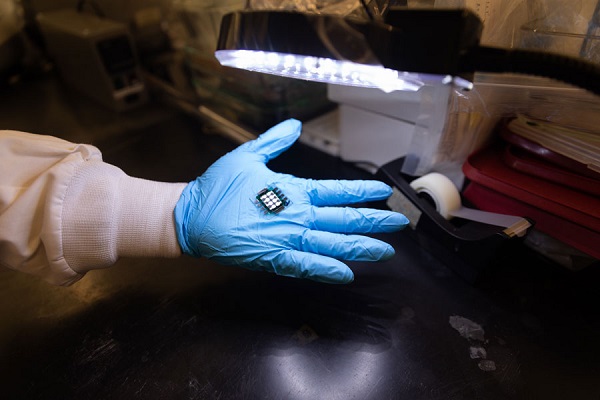
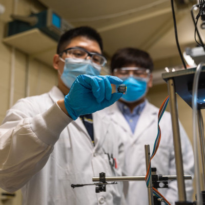
This prototype all-perovskite tandem solar cell measures one square centimetre and has a power conversion efficiency of 27.4%, which is higher than is currently possible with traditional single-junction silicon solar cells.
The tandem design enables the cell to produce a very high open-circuit voltage, which in turn improves its efficiency. But the key innovation came when the team analyzed the interface between the perovskite layer, where light is absorbed and transformed into excited electrons, and the adjacent layer, known as the electron transport layer.
“What we found is that the electric field across the surface of the perovskite layer — we call it the surface potential — was not uniform,” says PhD student Aidan Maxwell, another co-lead author.
“The effect of this was that in some places, excited electrons were moving easily into the electron transport layer, but in others, they would just recombine with the holes they left behind. Those electrons were being lost to the circuit.”
To address this challenge, the team coated a substance known as 1,3-propanediammonium (PDA) onto the surface of the perovskite layer. Though the coating was only a few nanometres in thickness, it made a big difference.
“PDA has a positive charge, and it is able to even out the surface potential,” says postdoctoral fellow Hao Chen, another of the co-lead authors.
“When we added the coating, we got much better energetic alignment of the perovskite layer with the electron transport layer, and that led to a big improvement on our overall efficiency.”
The team’s prototype solar cell measures one square centimetre in area, and produces an open-circuit voltage of 2.19 electron volts, which is a record for all-perovskite tandem solar cells. Its power conversion efficiency was measured at 27.4%, which is higher than the current record for traditional single-junction silicon solar cells. The cell was also independently certified at the National Renewable Energy Laboratory in Colorado, delivering an efficiency of 26.3%.
The team used industry standard methods to measure the stability of the new cell and found that it maintained 86% of its initial efficiency after 500 hours of continuous operation.
“Continuing to advance the efficiency and stability of next-generation solar cells is a crucial priority for decarbonizing the electricity supply,” says Professor Alberto Salleo, Chair of the Department of Materials Science and Engineering at Stanford University, who was not involved in the study.
“The team developed a deep chemical understanding of what was limiting a crucial interface — the junction with the electron-extracting layer — in the large-bandgap portion of perovskite solar cells. These insights from basic science, acted on with innovative materials engineering strategies, will continue to drive the field forward.”
The researchers will now focus on further enhancing efficiency by increasing the current that runs through the cell, improving stability, and enlarging the area of the cell so that it can be scaled up to commercial proportions.
The identification of the key role played by the interfaces between layers also points the way toward potential future improvements.
“In this work, we’ve focused on the interface between the perovskite layer and the electron transport layer, but there is another important layer that extracts the ‘holes’ those electrons leave behind,” says Sargent.
“One of the intriguing things in my experience with this field is that learning to master one interface doesn’t necessarily teach you the rules for mastering the other interfaces. I think there’s lots more discovery to be done.”
Maxwell says that the ability of perovskite technology to hold its own against silicon, even though the latter has had a multi-decade head start, is encouraging.
“In the last ten years, perovskite technology has come almost as far as silicon has in the last 40,” he says. “Just imagine what it will be able to do in another ten years.”
Read the original article on University of Toronto.