EV Group, a developer of wafer bonding and lithography equipment for the MEMS, nanotechnology and semiconductor markets, is partnering with DELO, amanufacturer of industrial adhesives, specified for wafer-level optics.
The partners are combining efforts to "enable novel optical devices and applications, such as biometric authentication and facial recognition, for the industrial, automotive and consumer electronics markets." The work will utilize a combination of EVG’s lens molding and nanoimprint lithography technology and DELO’s advanced adhesives and resist materials.
The work will be carried out within EVG’s NILPhotonics Competence Center at its headquarters in St. Florian, Austria, and at DELO’s headquarters in Windach, Germany. The NILPhotonics Competence Center provides an open access innovation incubator for customers and partners across the NIL supply chain to reduce development cycles and time to market.
Infrastructure includes cleanrooms and equipment supporting key NIL manufacturing steps such as step-and-repeat mastering, lens molding and EVG’s SmartNIL technology, as well as wafer bonding and required metrology. The partners presented the joint-development efforts at last week's SEMICON Europa, in Munich, Germany.
Supply chain collaborations
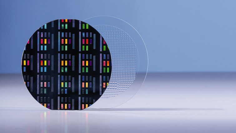
Advanced adhesives and resists play a key role in enabling wafer-level production of next-generation optical sensors for mass markets. The development of advanced optical materials requires extensive characterization of chemical, mechanical and optical properties as well as proven scalability for high-volume manufacturing.
This joint effort between EVG and DELO is intended to support both companies in refining their processes and products, as well as strengthening their expertise to address current and future market requirements. The partnership will also provide mature material and process know-how to speed up new product design and prototyping, supporting the roadmaps of both companies’ customers.
“The NILPhotonics Competence Center uniquely addresses the industry need for new ways to develop products with short time to market and the highest confidentiality,” commented Markus Wimplinger, corporate technology development and IP director at EV Group.
“Through partnerships with key players in the supply chain, such as DELO, we can operate even more efficiently as a central point to develop and establish decisive manufacturing steps for new production lines in close collaboration with process and equipment experts.”
“EVG and DELO are known as technology and market leaders in WLO and NIL equipment and, respectively, optical materials, with a proven track record in ramping these technologies and processes into high-volume production,” stated Robert Saller, managing director at DELO.
Applications for wafer-level optics
EVG's WLO manufacturing solutions enable various novel optical sensing devices for mobile consumer electronics products. Key examples include 3D sensing, time of flight, structured light, biometric authentication, facial recognition, iris scan, optical fingerprint, spectral sensing, environmental sensing and infrared imaging.
Other applications include automotive lighting, light carpets, heads-up display, in-car sensing and LiDAR as well as medical imaging for endoscopic cameras, ophthalmic applications and surgical robotics. EVG's WLO solutions are supported by the company's NILPhotonics Competence Center. DELO added that its multi-functional materials "are found in nearly every smart phone worldwide. With additional characteristics depending upon customers’ specific needs, these polymer materials are optimal for industrial environments with short cycle times where the bonding of tiny elements is needed."
Read the original article on Optics Org.