- Contents
- Abstract
- Solar Cell Manufacturing Technologies
Nanotechnology and Solar Cells
- Nanostructured Solar Cells
- 1. Perovskite Solar Cells
- 2. Dye-sensitized Solar Cells (DSSCs)
- 3. Quantum Dot Solar Cells
- 4. Polymer Solar Cells
- 5. Copper Indium Gallium Selenide (CIGS) Solar Cells
- 6. Copper Zinc Tin Sulfide (CZTS) Solar Cells
- 7. Cadmium Telluride (CdTe) Solar Cells
- 8. Gallium Arsenide (GaAs) Solar Cells
- 9. Amorphous Silicon (a-Si) Solar Cells
- 10. Tandem Solar Cells
- Nanotechnology-enabled Coatings
- Nanostructured Solar Cells
Abstract
Over the past decades, nanotechnology has played a pivotal role in improving the performance of first-generation silicon solar cells and laid the foundations for the new generations of solar cells based on thin films and nanostructures. Thus far, a wide variety of nanostructured solar cells have been introduced, but many scientists from around the world are still working to develop more and more efficient solar cells; perovskite, dye-sensitized, quantum dot, polymer, copper indium gallium selenide (CIGS), copper zinc tin sulfide (SZTS), cadmium telluride (CdTe), and gallium arsenide (GaAs) solar cells are cases in point. As for silicon solar cells, the main application of nanotechnology is to enable the development of antistatic, self-cleaning, and water-repellant thin films based on polyvinylidene fluoride or organosilanes to help improve their efficiency by reducing surface contamination. Since the major advances of solar technology have, directly or indirectly, their roots in nanotechnology, it appears that the future of solar power generation is, indeed, in the hands of nanotechnology.
1. Solar Cell Manufacturing Technologies
Despite our lives improving very fast, pollution remains one of the most pressing problems of modern times; thus, we need to decentralize power production from traditional grids sooner than later and turn to our only truly renewable energy source, the sun. Solar energy can be converted into electricity directly by photovoltaic effect or indirectly by using solar power concentrators. A great diversity of technologies are in use for converting the sun’s energy, which are mostly based on semiconductors. The National Renewable Energy Laboratory (NREL), the world's largest institute for testing the performance of various types of solar cells and modules to ensure the consistency and accuracy of photovoltaic performance measurements, has so far identified 25 types of solar cells that can be grouped into the following five categories shown in Table 1: multi-junction, single-junction gallium arsenide, crystalline silicon, thin-film technologies, and emerging technologies. These technologies can be industrialized depending on their capability of being mass-produced, module lifetime, and overall cost. Thus far, the highest efficiencies have been achieved by multi-junction, single-junction gallium arsenide, and crystalline silicon technologies, all holding dominant positions in the market today; but generally, these technologies are very complicated and more importantly costly. Hence, many researchers have recently turned to thin-film technology as well as emerging technologies (e.g., perovskite structures), due mainly to their lower costs and facile fabrication processes.
Table 1. The highest confirmed conversion efficiencies for research cells for a range of photovoltaic technologies, plotted from 1976 to the present, reported by the NREL on April 06, 2020 ∴
|
No. |
Photovoltaic Technologies |
Solar Cell |
Highest Confirmed Conversion Efficiencies |
|
1 |
Multijunction Cells |
Two-junction (concentrator) |
35.5 |
|
Two-junction (non-concentrator) |
32.9 |
||
|
Three-junction (concentrator) |
44.4 |
||
|
Three-junction (non-concentrator) |
37.9 |
||
|
Four-junction or more (concentrator) |
47.1 |
||
|
Four-junction or more (non-concentrator) |
39.2 |
||
|
2 |
Single-junction GaAs |
Single crystal |
27.8 |
|
Concentrator |
30.5 |
||
|
Thin-film crystal |
29.1 |
||
|
3 |
Crystalline Si Cells |
Single crystal (concentrator) |
27.6 |
|
Single crystal (non-concentrator) |
26.1 |
||
|
Multicrystalline |
23.3 |
||
|
Silicon hetreostructures (HIT) |
26.7 |
||
|
Thin-film crystal |
21.2 |
||
|
4 |
Thin-films |
Copper indium gallium selenide (concentrator) |
23.3 |
|
Copper indium gallium selenide |
23.4 |
||
|
CdTe |
22.1 |
||
|
Amorphous Si:H (stabilized) |
14.0 |
||
|
5 |
Emerging PV |
Dye-sensitized solar cells |
12.3 |
|
Perovskite solar cells |
25.2 |
||
|
Perovskite/Si tandem (monolithic) |
29.1 |
||
|
Organic cells (various types) |
17.4 |
||
|
Organic tandem cells |
14.2 |
||
|
Inorganic cells (CZTSSe) |
12.6 |
||
|
Quantum dots (various types) |
16.6 |
||
|
Perovskite/CIGS tandem (monolithic) |
24.2 |
2. Nanotechnology and Solar Cells
2.1. Nanostructured Solar Cells
2.1.1. Perovskite Solar Cells
Among various types of emerging solar cells, the ones based on perovskite have been the fastest to reach higher efficiencies, holding great promise for facile and low-cost production of solar cells, paving the way for clean energy generation by relying on the sun. Hence, emerging solar cells are still being extensively studied. The term perovskite refers to a large group of chemicals with the general formula of ABX3. Today, many researchers are attempting to develop more complex perovskite structures (e.g., organo-halide compounds) that show outstanding physical, optical, and electrical properties. These compounds have the general chemical formula of APbX3, where X represents monovalent ions such as fluorine, chlorine, bromine, and iodine. Several leading research teams have lately focused their studies on methylammonium lead halide perovskites with the chemical formula of CH3NH3PbX3, used as a 400-nm-thick light-absorbing layer in this class of solar cells. The other components of a typical perovskite solar cell are as follows (Figure 1):
1. a piece of glass coated with a 700-nm-thick layer of fluorine-doped tin oxide;
2. a blocking layer made of titanium dioxide (TiO2) in the crystalline phase of anatase with a thickness of 50 nm, used for preventing the charge recombination between the transparent conductive oxide substrate (e.g., FTO) and the perovskite layer;
3. a mesoporous layer composed of 20-nanometer TiO2 particles that acts not only as an electron transport layer but also as a scaffold for the perovskite layer. Al2O3, ZnO, and ZrO2 can also be used for preparing a mesoporous layer;
4. a hole transport material (HTM) with a thickness of 200 nm, for which Spiro-OMeTAD is widely used;
5. a back electrode (cathode) made of gold or silver with a thickness of 60 nm, which can also be replaced with other compounds such as carbon.
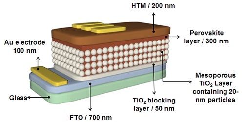
Figure 1. The components of a typical perovskite solar cell. ∴
Saule Technologies’ goal is to commercialize perovskite solar cells, especially for IoT applications. They employ an invented, unique method to produce solar modules by inkjet-printing perovskites on flexible foils. Saule’s perovskite technology for IoT aims to achieve longer device lifetime, higher bandwidth, data transmission with higher frequency, longer transmission range, smaller size, and improved security. They focus on B2B relationships and currently don’t serve individual customers. They are now equipping cleanroom, space for manufacturing, and storage, and they expect the initial efficiency to be around 10%. They are targeting a 50 EUR / m2 price for the solar cells by 2022. As a member of the international thin-film solar industry association (PVthin), they are dedicated to promoting perovskite photovoltaic technology with a focus on supporting a low-carbon economy, responsible product management, resource-saving production with sustainable raw materials and efficient PV recycling.
Swift Solar Inc. core technologies range from new solar cell architectures to specialized manufacturing techniques. They are now developing perovskite solar modules intending to achieve unmatched power-to-weight ratios due to their strong light absorption and high efficiency. New form factors for lightweight solar modules are enabled by ultra-thin perovskite films. Raw materials used in perovskite solar cells are produced in high volume at extremely low cost. Perovskites can be engineered to absorb different parts of the solar spectrum, enabling high-efficiency tandem solar cells.
2.1.2. Dye-sensitized Solar Cells (DSSCs)
At the heart of a dye-sensitized solar cell, lies a mesoporous layer composed of TiO2 nanoparticles with an average particle size of 20 nm, which is deposited on a piece of glass coated with a thin layer of FTO. The dye particles – commonly N-719 – are introduced onto the surface of the TiO2 nanoparticles and are responsible for injecting electrons into the system. A 50-nanometer-thick layer of TiO2 is placed between the mesoporous layer and the conductive substrate (FTO) to prevent the recombination of the photogenerated electron-hole pairs, and a piece of platinum-coated FTO glass is used as the back electrode (cathode); followed by injecting a liquid electrolyte between the anode and the cathode, which is generally based on iodide/triiodide (I ̄/I3̄) redox couple. The components of a standard DSSC are demonstrated in Figure 2. Acting as electrochemical cells, DSSCs convert solar energy into electrical energy through the following steps:
1. Sunlight passes through the FTO glass and hits the dye molecules on the surface of TiO2 nanoparticles.
2. Incident photons are absorbed by the dye molecules and excite their electrons. The excited electrons are transferred to the lowest unoccupied molecular orbital of the molecules, leaving the holes behind in the highest occupied molecular orbital (HOMO) of the molecules.
3. The excited electrons are then injected to the conduction band of the TiO2 electrode, and diffuse from TiO2 nanoparticles to the TiO2/FTO interface due to a concentration gradient, finally reaching the cathode (FTO) through the external circuit.
4. Since the dye molecules have been oxidized, they accept electrons from the electrolyte; in other words, the oxidized dye molecules are reduced to the ground state using I− ions of the electrolyte, leading to the formation of I3̄ ions. The resulting electrons are transferred to the HOMO of the dye molecules.
5. The remaining I3̄ ions diffuse toward the cathode where they are reduced to I− ions again. This step is accelerated by coating platinum on the counter electrode (cathode).
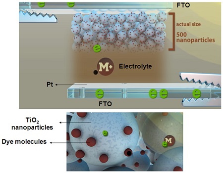
Figure 2. The schematic representation of the components of a DSSC. ∴
Solaronix SA has been a pioneer of dye-sensitized solar cell technology since its inception. They believe this type of solar cell demonstrates unmatched features that open solar technology to a host of innovative applications. Solaronix’s models offer some possibilities in terms of customization and integration, and come in a variety of colors and transparencies, offering unprecedented design flexibility for device or building integration. Their low light sensitivity makes them attractive for diffuse light conditions, including indoor applications. Since their goal is producing modules to be used in omnipresent machines and processes, while keeping manufacturing energy needs minimal, the energy payback time of their solar cells is reduced to a few months instead of several years. Solaronix’s demonstration DSSC can be used to power a low current motor, even in typical office light. Preferential pricing is available for the purchase of this cell, bundled with an electric motor or a model wind turbine.
G24 Power uses nanotechnology to deliver a huge step forward in the world’s ability to harness visible light into electrical energy through DSSCs. Their patented cells are thin, flexible, and lightweight which means that they can be used to power a wide variety of devices. G24 Power’s solar cells are suitable for shaded and diffuse light locations and work in a wide range of lighting conditions. They are produced using roll-to-roll techniques and can withstand flexing over 10000 times.
2.1.3. Quantum Dot Solar Cells
Quantum dots found their way into the field of solar cells for the first time when they were employed as a substitute for dye in DSSCs, creating a new class of solar cells called quantum-dot-sensitized solar cells that allowed for high-density electron injection and tuning the band gap. A wide variety of quantum dots have thus far been introduced for use in quantum dot solar cells such as lead sulfide (PbS), cadmium selenide (CdSe), and cadmium telluride (CdTe), which have opened the way to the development of Schottky, multi-junction, bulk heterojunction, and depleted heterojunction solar cells.
Solterra Renewable Technologies develops sustainable solar technology by replacing silicon wafer-based solar cells with high-production, low-cost, efficient, and flexible thin-film quantum dot solar cells. Until recently, the high cost of producing quantum dots made their use in solar cells prohibitive.
Quantum Materials Corp, the parent company of Solterra Renewable Technologies, has changed this paradigm with a new proprietary quantum dot production technology that dramatically reduces the cost of quantum dot production. This technology provides a simple and convenient method based on a self- assembly process that leads to the formation of microshells with spherical and non-spherical shapes. Next-generation quantum dot solar cell factories will use new thin-film flexographic roll-to-roll printing methods at a fraction of the capital expenditure of same-size silicon panel factories. This flexographic method enjoys various advantages such as the ability to potentially increase printing press speeds of up to 600 meters/minute with modern printers, large rolls that can be cut to finished size, low viscosity ink formulations for faster drying, and the ability to bond layers of the solar cell together in-line.
QD Solar is developing the next generation photovoltaic cells using colloidal quantum dot technology. These materials are nanometer-sized semiconductor particles whose bandgap can be tuned from the visible to the infrared by changing the particle size. The quantum dots are processed from solution, are compatible with high-throughput, cost-effective roll-to-roll processing technologies, and are inorganic, thus inherently more light- and air-stable than polymers.
NANO SOLAR INDIA produces transparent quantum solar panels for replacing glasses outside buildings, which are available in five different colors. The most paramount feature of these modules is that they do not require direct sunlight, and even the falling photons can generate electricity. They are mainly designed for construction applications such as outside vertical position glasses and transparent roofing glasses for inside skylight.
2.1.4. Polymer Solar Cells
Due to the capability of polymers to be deposited on flexible substrates without losing their properties, they enable solar scientists to design and build flexible solar cells. The components of polymer solar cells – shown in Figure 3 – are as follows:
1. a flexible substrate which is commonly made of polyethylene terephthalate (PET) foil;
2. a 150-nm-thick layer of indium tin oxide (ITO) as the anode;
3. a 40-nm-thick layer of PEDOT:PSS serving as an electron blocking layer which helps transport holes to the anode;
4. a 200-nm-thick layer of P3HT:PBCM, in which P3HT acts as the donor material and PBCM as the acceptor material;
5. an 80-nm-thick aluminum layer deposited as the back electrode.
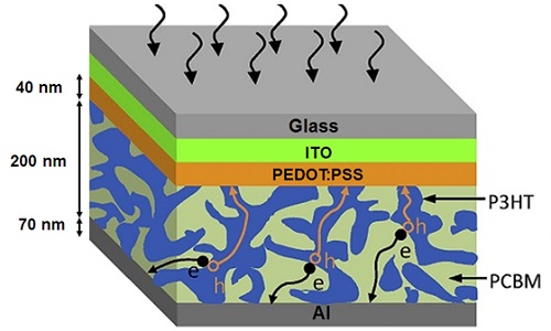
Figure 3. The structure of a typical polymer solar cell. ∴
Nano-C introduces a patented fullerene ink which is used in the production of organic photovoltaic (OPV). Fullerene acts as the n-type semiconductor or electron acceptor in OPVs. The n-type semiconductor is used in conjunction with a p-type material; either a polymer or another molecule as an electron donor. Typically, they are blended and cast as the active layer to create what is known as a bulk heterojunction. Fullerene is used on their own or derivatized (e.g., C60 and C70 PCBM) to increase solubility and modify electronic properties. The advantage of some embodiments of the invention is that the substituents used to derivatize fullerene can be chosen based on the calculated lowest unoccupied molecular orbital (LUMO) level or the calculated electron affinity. The goal in these embodiments can be to maximize the difference between the LUMO level of the n-type material with the Highest Occupied Molecular Orbital (HOMO) level of the p-type material, while still maintaining photo-carrier generation within the active layer.
2.1.5. Copper Indium Gallium Selenide (CIGS) Solar Cells
Copper indium gallium selenide (CuInxGa(1-x)Se2) is a p-type semiconductor that is used as the light-absorbing layer in CIGS solar cells – usually with a thickness of 2.5 mm. In addition to the CIGS layer, the following are the other major layers of this type of the cells (Figure 4):
1. a 500-nm-thick layer of molybdenum which is deposited on a piece of glass by sputtering;
2. a 40-nm-thick n-type buffer layer commonly made of cadmium sulfide (CdS);
3. a 50-nm-thick layer of intrinsic zinc oxide (i-ZnO) which protects the CdS and CIGS layers from sputtering damage while depositing the back electrode;
4. a 500-nm-thick layer of aluminum-doped ZnO (AZO) which is deposited as the back electrode.
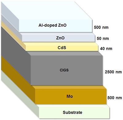
Figure 4. The schematic illustration of the components of a CIGS solar cell.
Ascent Solar introduces leading-edge CIGS photovoltaic technology on a flexible, plastic substrate, and its 30 MW nameplate production facility is in Colorado. Ascent is commercially producing CIGS cells on a plastic substrate with monolithic integration. With 48 Watts of solar power, the durable and compact Ascent XDTM48 Solar Charger is the ideal solution for charging today’s high-capacity power banks. This company employs a patented technology to provide power from dawn to dusk, even in cloudy conditions, in which four elements of CIGS uniformly deposited onto a roll of our flexible polyimide substrate. A very thin transparent coating is added to complete the semiconductor, and the roll passes through laser patterning and precision screen printing. The resulting modules are monolithically integrated. This provides multiple paths for current to flow around damage or shaded areas while continuing to operate.
Nanosolar Inc.’s new proprietary, next-generation CIGS Print2Power™ technology platform, enables the technology roadmap to increase power conversion efficiencies to 16 percent. Although this family of modules has yet long a way to potentially surpass current c-Si efficiency rates, this reduces total costs and provides new applications. Moreover, the Nanosolar Utility Panel’s innovative design significantly reduces balance-of-system costs through less mounting hardware, electrical cabling, and installation labor. Technological innovation on solar cell level includes:
- use of a highly conductive, low-cost aluminum foil as the substrate and bottom electrode of the cell
- CIGS ink with pre-defined ratio and a high-yield, high-throughput printing process to form an electronic-grade CIGS semiconductor
- novel Metal-Wrap-Through (MWT) back-contact design based on high-throughput foil lamination
- thin/printed transparent top electrode
The result of the front-end cell production is a roll of inexpensive aluminum foil substrate coated with multiple thin-film layers totaling less than two microns. These printed CIGS solar cells and panels are on track to reach efficiencies competitive with crystalline silicon panels in the next several years.
As a manufacturer of CIGS solar modules, AVANCIS Gmbh aims to offer extremely high standards of quality, reliability, and corporate responsibility that are exceptional in this dynamic industry. Their modules enjoy an excellent low-light performance, since they have the widest spectral sensitivity of any PV technology, demonstrated by their performance with cloudy skies, diffuse light or flat position of the sun. As a consequence of their subtle dark appearance and smart product design, the non-reflective modules blend seamlessly into their respective surroundings. Thanks to Kromatix™ patented technology, colored glass can be applied on SKALA solar panels. Colored SKALA solar panels generate nearly the same amount of energy as black SKALA panels with a small loss of efficiency. Compared to conventional colored solar panels, the SKALA KROMATIX™ panels use the reflection of the sunlight to generate their colored appearance. The multilayered treatment of the Kromatix™ front glass is designed to reflect a narrow spectral band of the visible light, in order to provide a color, the rest of the solar spectrum is being transmitted to the solar device and converted into energy.
FLISOM Flexible Solar Modules’ proprietary CIGS thin-film technology combines energy efficiency, high throughput manufacturing with advanced module design. The roll-to-roll production of modules of monolithically-integrated solar cells leads to panels’ expectation quality. Flisom's key technologies lie in the deposition of the CIGS semiconductor compound on flexible foil, laser scribing, and the design of flexible solar modules. The complex patterns of solar cells and other components can be designed and interconnected on a single sheet of plastic without having to add external hardware components.
Thanks to the integration of the world-record-breaking CIGS technology into the production, Solibro Gmbh modules are among the most efficient products of their kind, with the efficiency of up to 16%. The cell design of the Solibro thin-film modules minimizes the probability of shading of whole cells and therefore ensures you an optimum yield regardless of the position of the sun.
SoloPower Systems Inc. produces flexible CIGS modules optimized for sixteen-inch standing-seam metal roof integration. The modules are easily configured for multiple adhesive applications, enabling rapid installation and low-cost system integration with a wide variety of metal substrates. They have various advantages such as light-weight, non-penetrating mounting solutions, low-sun-angle, low-light performance under shade conditions, moisture barrier front sheet, sealed junction box, protective back sheet, and long life-time.
MiaSolé Hi-Tech Corp. is another company focusing on depositing CIGS films on a thin stainless-steel sheet. The sheet is then cut into cell form, covered with the ultra-wire interconnect and tested. Not only is it the highest efficiency thin-film cell, it is lightweight, flexible, and low-cost, and the shape can be modified to fit any form factor.
2.1.6. Copper Zinc Tin Sulfide (CZTS) Solar Cells
The mechanism and general structure of CZTS solar cells are similar to those of CIGS cells, except that the light-absorbing layer is replaced with CZTS with the chemical formula of Cu2ZnSnS4. What makes this class of solar cells stand out is that the toxicity of CZTS is lower than CIGS and its elements are abundant in nature.
2.1.7. Cadmium Telluride (CdTe) Solar Cells
In this group of solar cells, the light-adsorbing layer is a 10-mm-thick layer made of cadmium telluride as a p-type semiconductor. According to Figure 5, the components of a CdTe solar cell are as follows:
1. a 10-mm-thick layer of CdTe as a p-type semiconductor;
2. a piece of ITO-coated glass as the front electrode;
3. a 100-nm-thick layer of polycrystalline cadmium sulfide (n-type semiconductor) serving as a window layer;
4. a 50-nm-thick Al or Au layer deposited as the back electrode.
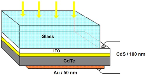
Figure 5. The layered structure of a CdTe solar cell. ∴
Toledo Solar is the manufacturer of CdTe thin-film photovoltaics for both residential and commercial rooftop markets, which offers an industry-leading 25-year warranty with simple and robust support for installers and homeowners alike. Its hermetically sealed, frameless all-glass construction creates the most beautiful and long-lasting solar panels on the market today. They feature an all-black and all-glass design and utilize the entire visible light spectrum. CdTe panels perform better than Si panels in warm and hot climates, and outperform Si panels in shaded and cloudy environments. Toledo Solar’s includes a glass substrate having a transparent conducting layer, such as tin oxide. A layer of cadmium sulfide is deposited onto the conducting layer by RF sputtering, which may be heavily doped to minimize ohmic losses.
WCP Solar has devoted its entire researching team in designing and producing thin-film PV modules that fit the requirements of construction environments. Their CdTe modules have uniformity color- pure black which provides an excellent appearance, fit best in buildings that have higher standards on appearance, unity and energy-independence. These CdTe thin-film modules have high efficiency and a proven-excellent record on power generation performance. Comparing to the crystalline silicon solar module, CdTe thin-film module generates 5-10% more in an average of electricity every year. To absorb the same amount of light, the thickness of the cadmium telluride film is only one hundredth that of the silicon wafer. The elongated cells of CdTe thin-film module help to reduce the hot spot effect of modules, which leads to a great advantage of improving the power generation capacity, ensuring the safety in usage and product life.
2.1.8. Gallium Arsenide (GaAs) Solar Cells
Due to their high production cost, high-efficiency gallium arsenide solar cells are mainly used in aerospace applications. Single-crystallin thin films of n-type and p-type GaAs are the main component of this class of the cells, for which numerous layered structures have so far been proposed; one of the commonest structures is shown in Figure 6.
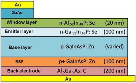
Figure 6. The components of a GaAs solar cell. ∴
GaAs is commonly used in single-junction solar cells (e.g., GaAs, InP, and InGaP), double- junctions (e.g., InGaP/GaAs), triple-junctions (e.g., InGaP/GaAs/Ge, InGaP/GaAs/InGaAs, and InGaP/GaAs/InGaAsNSb), four-junctions, and more.
Sol Voltaics AB provides next-generation solar nanotechnology solutions that can significantly enhance the efficiency and power output of solar panels at prices competitive to crystalline silicon. This company produces a patented lightweight photonic film, namely SolFilm™, consisting of high-efficiency gallium arsenide PV nanowires, which offers module manufacturers a low-cost, drop-in solution to boost conventional PV module efficiencies by 50% via ultra-high efficiency tandem modules. Manufactured through their Aerotaxy® process, SolFilm converts high energy sunlight directly into power and is transparent for infra-red light. The infra-red light can be converted into power by an underlying CIGS or silicon cell in a stacked configuration, enabling a far greater power conversion efficiency than found in current leading-edge conventional modules. By adding SolFilm™ on crystalline silicon modules, they convert today's average panel of 15.5 percent conversion efficiency to go beyond the silicon limits of 23-24 percent. Nanowires concentrate the sunlight without the use of optics or mechanical components. The nanowires just cover a small percentage of the surface area of a solar cell to gain substantial increases in efficiency.
NanoFlex Power Corporation aims at reducing the production cost of GaAs solar cells by enabling the most expensive component of the manufacturing process, the GaAs parent growth wafer, to be reused multiple times rather than being discarded after only a few uses. The GaAs cells produced from subsequent cycles maintain the same ultra-high-performance characteristics as those from the initial cycle. Its proprietary process also enables ultra-high-performance GaAs solar materials to be available on flexible and lightweight thin-film materials for use in a much wider variety of applications. They employ a method for integrating a thin-film solar cell with non-tracking mini-concentrators, as follows:
1) depositing at least one protection layer on the growth substrate;
2) depositing at least one sacrificial layer on the protection layer;
3) depositing a photoactive cell on the sacrificial layer, wherein the photoactive cell is inverted; and forming a patterned metal layer comprising an array of mesas on the photoactive cells by a photolithography method.
4) after forming the array of mesas, the method comprises bonding the patterned metal layer to a metalized surface of a plastic sheet, and etching the sacrificial layer with one or more etch steps that remove the photoactive cell from the growth substrate to form thin-film solar cells.
5) the method then comprises fabricating compound parabolic concentrators from a plastic material using at least one thermoforming process, and transferring the thin-film solar cells onto the thermoformed compound parabolic concentrators by an adhesive-free bonding step to form an integrated thin-film solar cell and compound parabolic concentrator.
NanoAvionics is working on the development of high quality and performance GaAs Solar Arrays for the growing small satellite market. Products address the most significant factors of price, durability, reliability, integrity, and lead time. The company’s goal is to make small satellites affordable to a wide range of companies and organizations around the globe expanding small satellites capabilities. NanoAvionics GaAs solar arrays are made of high-performance triple junction space-grade solar cells having GaInP/GaInAs/Ge epitaxial structures that enable missions with high power requirements. These solar cells reach up to 28.7 % efficiency and 36.85 mW/cm2 power generation capacity in LEO (AM0), and have an integrated by-pass diode to protect in series connected solar cell string from shadowing effects. These solar cells are assembled using NASA qualified low outgassing adhesive materials in a cleanroom environment.
Nano Solar India produces high-efficient GaAs solar panels which generate more energy over the lifetime of your system than other panels. Gallium arsenide is made into a cylinder first and then that is sliced into cells. Solar cells are then connected to the rest of the power network. Solar concentrators, made of clear plastic, are placed above them to focus the Sun’s rays.
Toyota Motor Corporation shows off solar Prius with 860 W output from 34% efficient cells. The car will be road tested at Toyota City in Japan. Solar charging technology for the vehicle will then be further optimized before the vehicle goes on sale. The car has large portions of its surface covered in indium gallium phosphide (InGaP), gallium arsenide (GaAs), and indium gallium arsenide (InGaAs) triple-junction cells. Now though, Toyota has returned to the concept and begun road testing a new generation of solar improved Prius. This time Toyota collaborated with Sharp Corporation and the New Energy and Industrial Technology Development Organization (NEDO) for a different cell tech that purports. The cell was developed in 2016 by Toyota’s two partners. The result can charge the vehicle battery while driving rather than just while stationary.
Read more:
Toyota shows off solar Prius with 860 W output
AZUR SPACE Solar Power GmbH offers highly efficient space solar cells, starting from the 28% class and ending in the high-end cell class of 32% -Advanced. All solar cells include the latest triple /and quadruple junction technology, where GaInP/GaAs/Ge layers are grown on a Germanium substrate and the whole product range benefits from many years’ experience on the space market. AZUR SPACE has already delivered over 1.5 million triple-junction GaAs solar cells to a wide range of customers.
Centro Elettrotecnico Sperimentale Italiano Company (CESI) produces standard triple-junction space cells (InGaP/InGaAs/Ge) with a typical efficiency of 30%. They are qualified for both Low Earth Orbit (LEO) and Geostationary Orbit (GEO) satellites according to standard ECSS E ST20-08C (see datasheet CTJ-30 below). CESI has made more than 200,000 solar cells that have powered more than 70 civil satellites for clients from over 25 different countries. These solar panels enjoy very low solar cell mass (81-89mg/cm2), thickness of 150µm ± 20µm, high radiation resistance, good mechanical strength, and high flexibility to customization.
MicroLink’s triple-junction inverted metamorphic (IMM) solar cells for space applications are manufactured using our state-of-the-art epitaxial lift-off (ELO) technology. The cells have an AlInGaP/GaAs/InGaAs structure and are grown using metalorganic chemical vapor deposition (MOCVD) on a GaAs substrate. The efficiency of the cells is 29% under AM0 illumination. Because of the ELO process, the cells are very light, with an areal mass density of <350 g/m2.
Spectrolab Inc. offers a range of GaInP/GaAs/Ge lattice matched solar cells with efficiencies reaching 32%. Spectrolab's space solar cells can be purchased as bare cells or assemblies complete with space-qualified coverglass, bypass diode, and interconnects for welded connections between solar cells (CICs). Based on a customer's specifications for maximum area, operating temperature and voltage, and the mission environment and duration, Spectrolab engineers maximize performance for End of Life performance. The panel substrates onto which Spectrolab's multi-junction circuits are bonded and wired to terminations, are provided as customer-furnished equipment.
Innovative Solutions In Space’s GaAs triple-junction solar cells are produced to meet customer needs in the field of small satellites and provide a full turn-key solution for those in need of a space mission, involving satellite systems in the range of 1 to 30 kilograms. These panels are mounted on aluminum or carbon panels include coarse sun sensors and temperature sensors designed for LEO missions.
Hanergy Thin Film Power Group Limited uses Alta Devices’ GaAs solar modules to produce solar-powered aircrafts, called Solar UAV. The wings of a small-scale UAV are generally 1 to 3 meters in length. Power plant and airborne equipment (balancing devices, cameras, communication and telemetry devices) are powered completely by cells. The high-altitude long-endurance UAV is used for military operations and has the advantages of fast speed, high altitude, and instant video signals provided. It adopts a wide-field-of-view lens, or wide-beam scanning radars to monitor dynamic movements of motorcade and people in movement, open deserts, and activities for targets on the sea, providing statistics and differentiation of tactical information over a wide range. The UAV has huge wings, easy for the pavement of efficient GaAs components, providing complementary electricity for fuel cells. Hanergy's 4.4 m fixed-wing UAV uses thin-film solar cells, extending the endurance between 6 to 10 hours and the scope of work reaching 400 to 700 kilometers. It is the world's most enduring industrial solar UAV, can be widely used in the military, civilian and commercial markets, including for oil and gas pipeline patrolling, agricultural monitoring, military police patrolling, disaster and emergency rescue, aerial photography and land surveying, natural resource testing, border and coastline patrols, and mining monitoring.
2.1.9. Amorphous Silicon (a-Si) Solar Cells
The role of nanotechnology in the fabrication of amorphous silicon solar cells is to create p-i-n junctions using n-type and p-type silicon layers with thicknesses of under 20 nm. As illustrated in Figure 7, a 300-nm-thick layer of intrinsic silicon, a 150-nm-thick layer of ITO, a 200-nm-thick layer of aluminum-doped ZnO (AZO), and lastly, a 300-nm-thick layer of silver as the back electrode are the other layers of a typical a-Si solar cell. The thickness of amorphous silicon solar panels can be designed to reach up to 300 times less than that of crystalline silicon solar panels. Generally, thin layers of a-Si are synthesized by vapor deposition techniques, among which plasma-enhanced chemical vapor deposition (PECVD) is widely used.
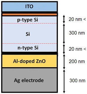
Figure 7. The schematic structure of an a-Si solar cell. ∴
With the cutting-edge technology and manufacturing experience, NanoPV Technologies Inc. offers turnkey solutions thin-film silicon solar panels. This company uses specific technology to increase the average cell efficiency of photovoltaics up to 17.6% for residential rooftop systems, on/off-grid commercial systems, and on/off-grid utility system applications. This technology includes:
- a thin film coating on a transparent substrate includes an effective amount of nanocrystalline silicon embedded in a matrix of amorphous silicon,
- a transparent conducting oxide layer on a layer of non-conductive transparent oxide provides light-trapping capability as well as electrical conductivity,
- an improved sputtering process and an improved RF plasma-enhanced CVD manufacturing method using high levels of hydrogen in the hydrogen-silane mixture and high electrical power levels for the plasma to increase the speed and to lower the cost of manufacturing.
Kaneka offers a new structure of tandem solar modules. Its dual-layer structure of microcrystalline and amorphous thin-film silicon can capture from short to long wavelengths of the light spectrum, allowing this panel to convert even more sunlight into electricity. Unlike traditional crystalline panels, the thin-film silicon cells allow it to perform even if part of the panel is shaded. In addition, modules can be installed close to each other and in low angles allowing more roof coverage.
Panasonic Solar Amorton Co. produces amorphous silicon solar cells with a variety of voltages, shapes, and forms. Their production method allows other substrates, such as stainless steel or plastic films, to be used instead of customary glass substrates. This means that previously unknown solar cells can also be created, including solar cells that are round, square, or any other complex shape or solar cells that can even be bent. It is also possible to create areas in these solar cells that just consist of transparent glass by etching. The human eye is sensitive to light from a range of about 400 to 700 nm wavelengths. Since amorphous silicon solar cells are sensitive to light with essentially the same wavelengths, they can also be used as visible light sensors.
WSL Solar Co’s amorphous solar cells have good performance during weak light condition and can be used to power low-consumption electronic devices such as watches, calculators, measurement units, wireless sensor, and weather station. Solar cell with thickness 1.1 mm can be easily embedded into plastic holders.
2.1.10. Tandem Solar Cells
Tandem solar cells have been introduced as an innovative solution for increasing the efficiency of solar cells by splitting the spectrum using a solar cell that is optimized to each section of the spectrum. The most common tandem configuration is to grow them monolithically so that all the cells are grown as layers on the substrate, in which individual cells are connected by tunnel junctions. A variety of tandem cells such as DSSC/c-Si, a-Si/DSSC, perovskite/c-Si (mechanically stacked tandem), perovskite/c-Si (monolithic tandem), and CZT/c-Si (CdZnTe is a member of thin-film solar cell family) has been introduced.
Oxford PV exclusively focuses on developing and commercializing a perovskite/silicon tandem solar cell technology. They are building the world’s first volume manufacturing line for perovskite-on-silicon tandem solar cells. Solar panels built with Oxford PV’s perovskite solar cell technology will generate more power, critical for delivering more affordable clean energy, accelerating the adoption rate of solar, and addressing climate change. Since 2016, the facility has supported the transfer of technology from their labs to industrial equipment and processes, in preparation for mass production. This has been supported by a development partnership with a large manufacturer of silicon solar cells and modules.
2.2. Nanotechnology-enabled Coatings
2.2.1. Antistatic, Self-cleaning, and Water-repellant Coatings
In the field of silicon solar cells currently available on the market, a wide range of benefits enabled by nanotechnology can be observed. For instance, this leading-edge technology has laid the groundwork for the design and development of antistatic, self-cleaning, and water-repellant thin films. Solar panels are usually exposed to dust, soiling, bird droppings, rain, snow, air pollution (chemicals such as sulfur dioxide, carbon monoxide, lead, and nitrogen oxides), etc., and the accumulation of these kinds of debris on the panels over time degrades their performance by blocking the light transmission to their absorbing-layer. Only 4 g of soil covering per square meter of solar panels can decrease their efficiency by up to 40 percent. Cleaning the panels, however, is not the ultimate solution to this problem, because a considerable amount of detergent should be applied to the panels by hand, thus consuming a large amount of water, manpower, and time. Furthermore, detergents can corrode the panels and damage them in the long run. That’s why extensive research has been underway and many companies are turning to the use of nanotechnology-based solutions, which not only are highly cost-effective but also do not impair the panels. These solutions lead to the formation of a thin film – under 100 nm in thickness – on the surface of solar panels that protects the panels, thereby increasing their efficiency as well as their lifetime. It should be noted that using this type of solutions does not obviate the need for cleaning the panels, but rather facilitates and accelerates the cleaning process and helps the panels stay clean for longer periods. Reducing maintenance costs, improving the abrasion resistance of the panels, and enhancing their durability are also other benefits of using these solutions. Polyvinylidene fluoride (PVDF), organosilanes, and semiconductors such as TiO2 are widely in use to serve this purpose.
Innovative Nano Technology LLC, taking a role in the field of nanotechnology-based coatings, produces a specific water-resistant coating, which is only around 100 nanometers (15-30 molecules) thick. This liquid spray consists of almost pure silicon dioxide nanoparticles extracted from quartz sand. This product is used to protect solar cells from getting dirty. Weather conditions highly affect the efficiency of panels. Particles of dust and sand can greatly decrease the performances of modules. Maintenance costs are thus very high and require specific tools and special care so that the cells are not damaged by the process. By applying this coating, harsh cleaning is less required and maintenance can be achieved on a frequent basis with the use of water due to the easy-clean effect brought by this long-lasting refinement on the cells.
Solar Armour delivers easy-to-apply, self-cleaning, hydrophobic, and invisible solar panel coating using advanced silane coupling agents and the purest silicate particles to make sure a long-lasting durable layer of protection. It enjoys the durability of around ten years. The self-cleaning glass effect keeps PVs clean, maintaining efficiency, and significantly reducing the need for expensive cleaning. It also repels water molecules more quickly than non-coated hydrophilic surfaces. It is highly resistant to salty air such as coastal areas and reduces the growth of micro-organisms and bacteria. Moreover, this product stops bird fouling and tree sap from sticking to the exterior.
Swedish Algae Factory produces a new solar shield aided by a group of algae, called diatoms, which are encapsulated by a nanoporous mechanically stable silica frustule. The silica frustule constitutes of three layers of nanoporous material. Each layer has its specific nanopore size. The top layer has a larger nanopore size and the inner layer has the smallest nanopore size. The pores in the different layers are intertwined through channels in a funneled structure. These funneled channels are naturally designed to transport necessary nutrients and light into the algae cell in an efficient way. It has been shown that by adding a diatom frustule layer on top of silicon-based solar panels the efficiency of the solar panel can be enhanced significantly, by more than 4% in lab tests. When adding the material into a future type of solar panel (DSSC) the efficiency of that solar panel was enhanced by 60% in lab tests. Its unique structure was also evolutionarily developed to block UV light, which makes the material interesting for use as a UV filter in plastics and sunscreens.
Solargenome produces a collection of bags and accessories equipped with solar panels to generate electricity from light. Each product is fitted with a solar panel that is used to charge a lithium battery that can, in turn, be used to recharge your portable electronics. This patented technology employs photoreactive materials containing conductive polymers and nano-engineered materials to provide tough, waterproof, lightweight, and flexible panels which react with both indoor and outdoor light.
Other companies are also producing solar shields using SiO2, TiO2, and polyvinylidene fluoride (PVDF) nanostructured materials, among which mention can be made of Nano Solutions, Percenta Nanotechnology, PURRATIO AG, CSG Holding Co., Joma International AS, ARL Designs LLC, Triton-Nereid, Halo Energy Ltd, NADICO Technologie GmbH, DryWired, BFP hellas, Balcony Systems Solutions Ltd, Heliotex LLC, Olympus, tuVapor, NanoSafeguard, Nanobase Kft, Nanotech Products Pty Ltd, Unelko Corporation, WINSOL Laboratories, Nanopower International LLC, and NanoMagic.
2.2.2. Magnesium-fluoride (MgF2) Anti-reflective Coatings
The high reflection coefficient of the materials used in the fabrication of solar cells prevents them from reaching their true potential in terms of efficiency and the problem even worsens for silicon and CIGS solar cells; applying anti-reflective coatings onto the panels is a way around. As a material with a significantly low reflection coefficient, magnesium fluoride shows great efficiency on the wavelengths of light ranging from 120 to 900 nm, and is commonly coated on the top surface of solar cells using vapor deposition techniques to form a layer with a thickness of 70 to 120 nm. Titanium dioxide, zinc sulfide, and silicon nitride are other materials employed as anti-reflective coatings in the solar industry.
2.2.3. Nano-coated Silicon Solar Cells
Solaxess SA has succeeded in developing nanotechnology-enabled films that can be integrated into the manufacturing process of solar panels to scatter the whole visible spectrum while transmitting infrared light, giving the panels a colorful appearance; architects will no longer have to sacrifice the beauty of the buildings they design for the use of solar energy and the company thus puts an end to the ugly solar-powered buildings era. From an aesthetic standpoint, classical photovoltaic panels do not satisfy customers due to their appearance, being in unattractive blue-black color. Therefore, it stands to reason that many architectures are reluctant to integrate them into their construction design. The company offers the manufacturers of photovoltaic modules with various custom-made white films and colored films, helping them meet demands for individualized customized designs. This film is either applied on top of an existing module or integrated into a new module during assembly. The company’s products are introduced based on three patents (EP3184994A1, EP2684839A1, and US7755835B2) granted by the Swiss Center for Electronics and Microtechnology (CSEM), which develops know-how and high-end equipment and processes for cell and module metrology and related characterizations, which are transferred to its industrial partners. The method consists of a plurality of layers, to highly reflect visible light while transmitting infrared. The scattering of the visible light, necessary to give a white appearance to a mirror-like surface is achieved by growing the filter on a micro-structured surface. The result is a white homogenous surface. Other color approaches are achieved by adapting the combination of the filters.
Read more:
Buildings Can Now Be both Solar-powered AND Aesthetically Pleasing
Jiangsu Runner PV Technology Co. is also active in manufacturing colored solar photovoltaic cells and modules. This lightweight and frameless module, which is fire-resistant, is produced by the ESS spraying technique.
Evolution Solar Inc. sells graphene-coated solar panels which are designed to absorb sun rays and convert them into electricity. Solar panels made of solar cells which are coated with thin-film of graphene are called graphene-coated solar panels. Graphite can be used to redefine electricity generated through solar panels. The new graphene film helps in creating electricity using raindrops. When creating electricity from sunlight, the graphene-coated solar panels work in as much as the same way as the traditional panels that are laid out on rooftops in many homes and workplaces does. But when the sun hides behind the clouds and it is raining, it is then that the graphene-coated cells in the panel become active. Graphene separates the ammonium, calcium, and sodium ions in the rain from the water. These ions stick to the electrons in graphene creating a dual-layer pseudo-capacitor system which generates electricity.
