Graphenea has announced the launch of a new product – highly flat monolayer graphene. The graphene is grown by CVD on copper thin film on a 2” sapphire substrate. With extremely low roughness that is less than 4 nm, this new product is targeted at applications in photonics, high-performance electronics, magnetic memory, and freestanding membranes.
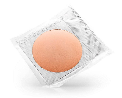
The product aims to meet wafer-scale integration requirements to build uniform graphene devices in a fashion compatible with current industrial fabrication methods. The flat graphene product is ready to be transferred by electrochemical delamination or dry methods since the sapphire substrate is robust enough to withstand mechanical damage, preventing tearing and wrinkling of the thin Cu sheet. The total wafer thickness is 430 micrometers. Full product information can be found in Graphenea's online store.
Read the original article on Graphenea.