Nanostructured and nanopatterned surfaces are an integral component in many nanotechnological applications. Easy to use and economical, the method of nanoimprinting has great potential for applications such as high-density data storage, photonic devices, holograms, bio-nanofluidic chips, water filtration, and electrodes in fuel cells. However, the precision of replication is limited in most materials due to those materials’ atomic structures.
In APL Materials, Schwarz shows that when working with metallic glasses, there’s virtually no limit to the accuracy that you can have when replicating surface features. In fact, the level of precision reaches down to the subatomic level. The key is the atomic structure of the materials. Unlike crystalline materials, which have atoms that are specifically arranged, atoms in glasses are arranged without restrictive periodic order principles.
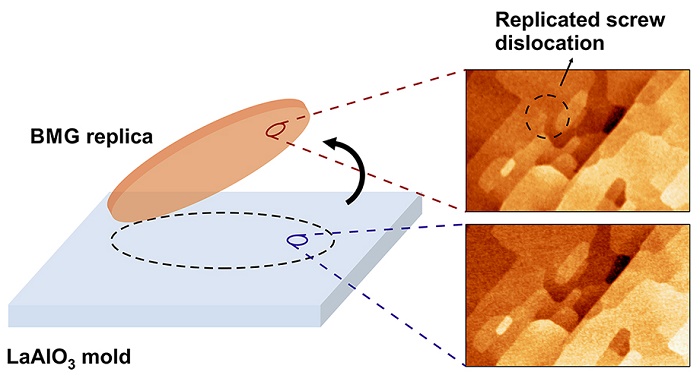
“Crystals always want to put atoms in specific places, and if your mold doesn’t match with that, you’re out of luck,” Schwarz said.
But metallic glasses don’t have such rigidly arranged atoms, allowing them to adjust to where they’re needed. By heating the glass, the researchers were able to weaken the material’s internal cohesion just enough to allow the atoms to move however way needed with near perfect accuracy.
“For the first time, we demonstrated that any structure you have, you can replicate it - the metallic glass will correctly conform to it,” he said. “You can do that with practically no limit in accuracy.”
That means they can provide an ideal platform for advancing research in the fundamental study of structure, deformation, and phase transitions of glasses as well as enabling novel applications in fields that make use of surface functionalization through topography.
In a second paper, in ACS Applied Materials and Interfaces, Schwarz also looks at nanofabrication of bulk metallic glasses, but with a different approach.
For that study, which received an “Editor’s Choice” designation by the journal, Schwarz developed a method based on magnetron sputtering. In magneton sputtering, gas ions, typically argon, are hitting a “target” and eject target atoms in the process. The ejected atoms then travel across vacuum to eventually reach a substrate on which they form a film.
Due to the wide range of alloys that can be used as targets and the large substrate areas that can be covered, the method provides researchers a large toolbox for selecting a desired surface chemistry while being extremely versatile in terms of size, shape, and the nature of the surface pattern and of the molds that can be used. Schwarz said it could effectively elevate atomic-scale replication from a “scientific curiosity” to a widely used nanofabrication tool.
During the replication process, the high degree of accuracy is based partly on the sputtering technique, but also decisively on the fact that the target alloys used to sputter the films do not crystallize. Because of this, there are no dimensional limitations from films that attempt to establish crystalline order.
“It shows that we can replicate surface structures down to sub-angstrom [less than one 10 billionth of a meter] on a large scale, and that this may open the way to use these materials on a large scale for the production of actual workpieces and for affordable prices,” he said.
Since only scarce amounts of material are needed, the new approach is economical. It’s also applicable to a vast array of alloys, flexible in the type of molds it can replicate, and can easily be scaled up. Potential applications of this new approach include the development of nanowires and nanotubes for nanoelectronic applications.
Read the original article on Yale University.

