Optoelectronics, a field of photonics that exploits quantum mechanical effects of light on electronic materials, in particular semiconductors, has gained a lot of traction for its promise in all sorts of applications. These range from solar cells and LEDs to colloidal lasers, a technology expected to replace conventional semiconductor laser diodes used in barcode scanners and fiber optic communications.
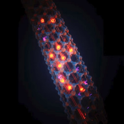
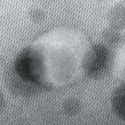
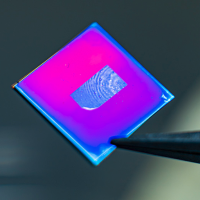
In the search for materials with better optical properties more suitable for use in optoelectronics, research has focused on nanoplatelets, which are highly promising low-dimensional semiconductor nanocrystals. These are flat structures, just a few nanometers in size, and remarkably versatile and tunable. Modern precision synthesis techniques allow researchers to grow them essentially on-demand, controlling their shape, thickness, and crystal structure. These parameters directly affect the photoluminescence capability and properties.
“Tailoring the synthesis of photoluminescent nanocrystals for specific applications may require predictions of spectral and relaxation characteristics. Hence, we need a detailed understanding and modeling of the underlying kinetics,” Skoltech Provost Keith Stevenson, professor at the Center for Energy Science and Technology and a co-author of the paper, explains.
Stevenson, PhD graduate Aleksandr Kurilovich and Vladimir Palyulin, Assistant Professor at the Center for Computational and Data-Intensive Science and Engineering, joined their colleagues in focusing on a way to explain non-trivial kinetics of semiconductor nanoplatelet photoluminescence in experiments. According to the researchers, earlier theoretical descriptions and experimental findings have always assumed an exponential decay of photoluminescence intensity in nanoplatelets. But more recent measurements showed a stark power-law behavior of the long-time, pointing to complexity.
The team built two models, a simulation one and a theoretical one, describing the kinetics of photoluminescence in nanoplatelets through the activity of excitons, quasiparticles in the semiconductor that are responsible for light emission in the case of their recombination. The models point to trapping of excitons at surface defects and its interplay with diffusion as key reasons for the complex kinetics. This allowed to successfully interpret experimental results from composite nanoplatelets made of cadmium selenide and cadmium sulfide.
“The model shows the importance of defects at long times and their ability to delay the recombination. This could be used to estimate the needed defect density for slowing down the emission, thus, extending the emission time,” Stevenson says.
The paper was published in the journal Physical Chemistry Chemical Physics. Other organizations involved in this research include Lomonosov Moscow State University, Institute for Physics & Astronomy at the University of Potsdam, and Akhiezer Institute for Theoretical Physics, National Science Center “Kharkov Institute of Physics and Technology”.
Read the original article on EurekAlert.