The first study, published in ACS Nano and led by graduate student Jothi Priyanka Thiruraman, postdoc Paul Masih Das, and professor Marija Drndić, shows the ionic transport properties of these pores, with promise for applications in water purification and desalination as well as for creating artificial pores that mimic ion channels in biology.
The second study, published in Science Advances, demonstrates how helium gas flows through these pores. This work was conducted by experimentalists at Penn and Radha Boya’s group at the University of Manchester with theoretical modelling by researchers at Shahid Rajaee University and the University of Antwerp.
Researchers in the Drndić lab have expertise making atomically-thin materials and devices that are dotted with nanopores, holes 100,000 times narrower than the width of a human hair. Wanting to scale these pores down even further, Thiruraman and Masih Das previously developed a method for making “angstrom-size” pores, ones that are small enough to only allow single atoms and small molecules to pass through. While this work was instrumental in demonstrating that these types of pores could be made, fabricating devices for use outside of controlled, experimental settings remained a challenge. “There’s a lot of device physics between finding something in a lab and creating a usable membrane,” says Drndić.
To get from fundamental discovery to a working device, Thiruraman and Masih Das synthesized materials with angstrom-sized pores while making systematic changes to their previous method to see how they could create a more resilient material. This process involves using a chemical vapor deposition chamber that flows gases over a substrate to grow the material atom by atom. Then, the single-atom-thick material is transferred onto a transmission electron microscope grid and exposed to either a focused electron or ion beam, which punches out single atoms and leaves behind tiny, atom-sized pores.
Using a systematic approach to testing and refining their fabrication process, the researchers were able to refine their method and develop a prototype that could be tested in more “real-world” conditions than was previously possible. “Instead of just studying the material inside of an electron microscope, how do you make an actual device? That’s something that took us a long time to figure out,” says Masih Das. “We used our knowledge to make devices that you can measure ionic or gas transport on, and that was the big difficulty.”
“Being able to reach that atomic scale experimentally, and to have the imaging of that structure with precision so you can be more confident it’s a pore of that size and shape, was a challenge,” adds Drndić. “That came with the advancement of the technology as well as our own methodology, and what is novel here is to integrate this into a device that you can actually take out, transport across the ocean to Manchester if you wish and measure.”
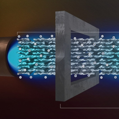
Prototypes in hand, the researchers ran experiments using salt water to see how effective the material was at removing salt ions from the water, those results were published in ACS Nano. “When you shrink the system to a single atom, we see that it’s independent of the salt water that you are putting in, so the hole does not seem to distinguish between what ion is going through,” says Thiruraman. “For salt ions, we are able to see with just a single hole a very standard saturated current level because the hole is so small, and its size dominates the conduction behavior.”

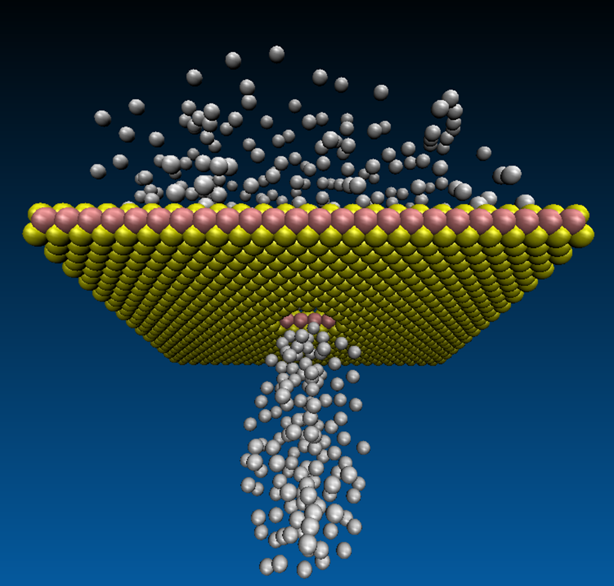
A diagram showing how the zero dimensional pores can also be used to filter gases.
Then, to see if the material could also filter gases, they collaborated with researchers at the University of Manchester who had previously developed a way to measure gas transport in nanoscale devices. This work, published in Science Advances, shows that their device can also be used to move helium atoms through atomic apertures and is the first-ever measurement of its kind. “We were very surprised to get any results at all because the holes are tiny,” Thiruraman says. “No one’s ever measured something like this, so just getting a helium atom to pass and detect through atomic apertures was very cool.”
The opportunities for potential applications are wide-ranging, from water desalination, energy harvesting, and measuring small molecules such as hormones and pharmaceuticals. “But of course, at this fundamental level, we’re trying to see how these materials are robust at the atomic scale,” says Drndić. The group is now interested in continuing its fundamental investigations of this material to better understand if the pores change over time, if layering individual sheets could change a material’s properties, and how the geometric shapes of the pores themselves influence transport mechanisms and device properties.
Drndić credits work done by Masih Das and Thiruraman, which includes mastering a broad range of techniques, spending a year developing methods, and testing numerous samples, as essential for both characterizing and creating these devices. When this work began, there were very few studies in this area at all, Drndić says. Now, this nascent field has dedicated conferences, a rich literature, and dedicated researchers from Penn who have been at the forefront since day one.
Read the original article on University of Pennsylvania.


