Over the past few years, researchers have been trying to develop new designs for perovskite solar cells that could improve their performance, efficiency, and stability over time. One possible way of achieving this is to combine 2-D and 3-D halide perovskites in order to leverage the advantageous properties of these two different types of perovskites.
The two-dimensional crystal structure of 2-D halide perovskites is highly resistant to moisture; thus, it could help to increase the performance and durability of solar cells with a light-absorbing 3-D halide perovskite layer. However, most of the strategies for combining 2-D and 3-D halide perovskites proposed so far simply entail mixing these two materials together (e.g., mixing 2-D precursors with a solution-based 3-D perovskite or reacting 2-D precursor solutions on top of a 3-D perovskite layer).
Researchers at Seoul National University and Korea University have recently devised an alternative approach for creating solar cells that combine 2-D and 3-D halide perovskites. This approach, outlined in a paper published in Nature Energy, could help to simultaneously improve both the efficiency and long-term stability of these cells.
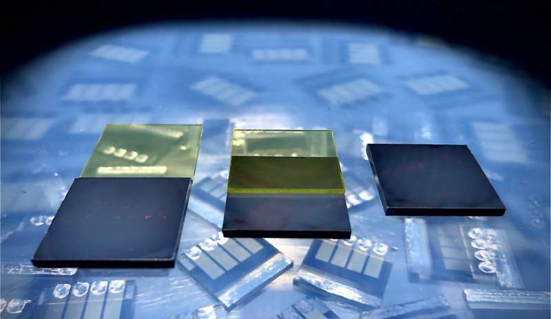
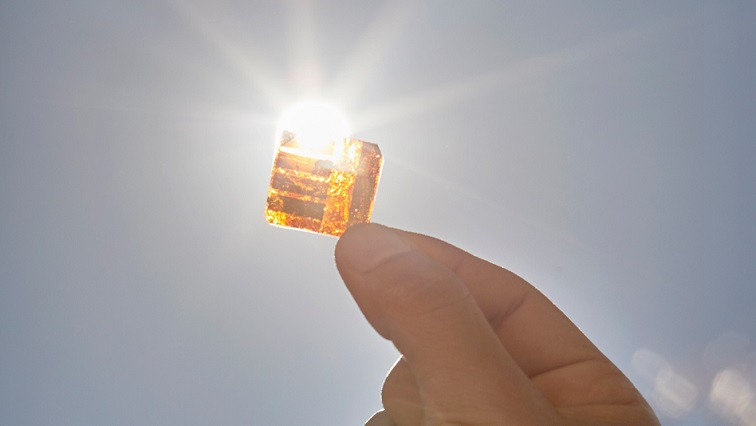
2D film, 3D film, stacked 2D/3D film, and SIG-processed 2D/3D film against the backdrop of the completed perovskite solar cells. Yellow transparent 2D perovskite BA2PbI4 film (top left), dark 3D perovskite film (bottom left), stacked 2D/3D film (middle), SIG-processed 2D/3D film (right). The SIG-processed intact 2D/3D junction could be obtained by applying heat and pressure into the stacked 2D/3D film. The 2D film is grown in an in-plane direction on top of the 3D film during the SIG process.
"Although the mixing of different perovskite films has some positive effect on efficiency and moisture stability, the 2-D formation through the solution process with the chemical reaction of the 2-D precursor with 3-D halide has limitations, such as vulnerability to heat and difficulty in implementing junctions for internal electric field design in the device due to an unintended quasi-2-D phase formation," Prof. Jun Hong Noh, one of the researchers who carried out the study, told TechXplore. "We have tried to solve this problem."
To overcome the limitations of previously proposed strategies for creating 2-D/3-D halide perovskite-based solar cells, Prof. Noh and his colleagues tried to create a suitable junction between a solar cell's light-absorbing layer (with a narrow bandgap) and the functional 2-D layer (with a wide bandgap). This functional layer is found in many existing high-efficiency solar cell structures, including gallium arsenide (GaAs) and heterojunction with intrinsic thin layer (HIT) silicon solar cells.
GaAs and HIT solar cells use a III-V semiconductor (AlGaAs) and amorphous silicon (a-Si), respectively, as a functional layer with a wide bandgap, in order to form a proper internal electric field. In these solar cells, the functional layer and the light-absorbing layer are typically homogenous. To design their solar cells, Prof. Noh and his colleagues thus made sure that they used a 2-D halide perovskite with a wide bandgap that was homogenous with the 3-D halide perovskite they selected.
"In order to form an intact 2-D/3-D junction, we came to the conclusion that the solution process should be excluded when forming the junction," Prof. Noh said. "That is how the solid-phase in-plane growth (SIG) process was born. In the SIG process, a 3-D film and a 2-D film are separately prepared, the 2-D film is stacked on top of the 3-D film so that they face each other, and then heat and pressure are applied to induce the 2-D film to grow on the 3-D layer."
Using this unique design strategy, the researchers were able to grow a highly crystalline 2-D film on top of the 3-D halide perovskite film without damaging it and without using solvents. This resulted in the formation of an intact 2-D/3-D junction.
Prof. Noh and his colleagues found that their approach does not lead to the unintended formation of a quasi-2-D film, which can sometimes occur when 2-D and 3-D halide perovskite films are mixed together. The resulting structure is thermally stable, while also allowing the researchers to easily control the thickness of the 2-D film and manipulate the 2-D/3-D junction's internal electric field.
"Our approach can simultaneously improve efficiency and long-term stability of perovskite solar cells," Prof. Noh said. "In addition, we presented a method to make the intact junction (halide/halide) between homogeneous halides, rather than the junction between heterogeneous materials (i.e., halide/oxides or halide/organics), which is the conventional device structure so far in perovskite solar cells."
The design strategy introduced by Prof. Noh and his colleagues could soon be used to create 2-D/3-D halide junction perovskite solar cells that have both a high efficiency and a high thermal stability. In the future, their work could also inspire other research teams to employ the same strategy or devise similar approaches to improve the performance of perovskite-based solar cells.
"In this recent study, we used butylammonium lead iodide (BA2PbI4), the simplest structure among 2-D halide perovskites," Prof. Noh said. "However, research exploring the application of new 2-D perovskites is underway for a better 2-D/3-D junction design. Through this, we hope that we will be able to implement a high-efficiency perovskite solar cell, such as GaAs."
Read the original article on TechXplore.

