The magnetic ‘spin’ of an electron is like a little bar magnet, whose orientation can be set with an applied magnetic field.
In materials with a ‘spin-orbit interaction’ the spin of an electron is determined by the direction of motion, even at zero magnetic field. This allows for all electrical manipulation of magnetic quantum properties.
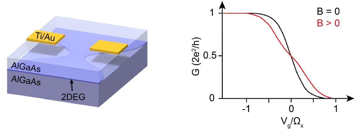
Applying a magnetic field to such a system can open an energy gap such that forward -moving electrons all have the same spin polarisation, and backward-moving electrons have the opposite polarisation. This ‘spin-gap’ is a pre-requisite for the formation of Majorana zero modes.
Despite intense experimental work, it has proven extremely difficult to unambiguously detect this spin-gap in semiconductor nanowires, since the spin-gap’s characteristic signature (a dip in its conductance plateau when a magnetic field is applied) is very hard to distinguish from unavoidable the background disorder in nanowires.
The new study finds a new, unambiguous signature for the spin-orbit gap that is impervious to the disorder effects plaguing previous studies.
“This signature will become the de-facto standard for detecting spin-gaps in the future,” says lead author Dr Karina Hudson.
REPRODUCIBILITY
The use of Majorana zero modes in a scalable quantum computer faces an additional challenge due to the random disorder and imperfections in the self-assembled nanowires that host the MZM.
It has previously been almost impossible to fabricate reproducible devices, with only about 10% of devices functioning within desired parameters.
The latest UNSW results show a significant improvement, with reproducible results across six devices based on three different starting wafers.
“This work opens a new route to making completely reproducible devices,” says corresponding author Prof Alex Hamilton UNSW).
THE STUDY
New signatures of the spin gap in quantum point contacts was published in Nature Communications in January 2021 (DOI 10.1038/s41467-020-19895-3).
As well as support by the Australian Research Council, funding was received from Germany’s Deutsche Forschungsgemeinschaft the UK’s Engineering and Physical Sciences Research Council and the Sydney Quantum Academy.

Quantum point contact structure (left) in which an applied voltage constricts electron movement to one dimension, with conductance (right) showing effect of applied magnetic field (red)
Semiconductor crystals were grown at the University of Cambridge and the Ruhr-Universitat Bochum. Devices were fabricated and examined at UNSW, Sydney. Theoretical studies were performed at the University of Massachusetts Boston and Ludwig-Maximilians Universität, München.
Read the original article on Arc Centre of Excellence in Future Low-Energy Electronics Technologies.


